



IntelliPaper
Abstract
Context: Many areas of modern electronic equipment, such as medical, automotive, portable, and special-purpose electronics, place increased demands on mass and volume. These devices often have irregular volume structures for accommodating electronic components. Therefore, 3D printed circuit boards are ideal for implementing such designs, and improving their efficiency, as well as optimizing the selection of mounting types, are pressing challenges.
Objective: The aim of this work is to develop a 3D printed circuit board method that is efficient in production and use, as well as a method for objectively selecting the optimal PCB option from the existing variety when designing miniature electronic equipment.
Method: The design and manufacturing method for manufacturing rigid-flexible printed circuit boards is based on traditional PCB manufacturing methods with an appropriate addition that allows for the achievement of three-dimensional design properties.
The method for selecting a 3D printed circuit board option consists of two parts: a heuristic method and passive game theory.
Results: A design and engineering method for producing a rigid-flexible printed circuit board has been developed. Its main feature is its fabrication on a single base—a rigid printed circuit board.
A sequence of steps for implementing a heuristic method is presented, and 3D printed circuit assembly metrics and their characteristics are developed, serving as input for experts selecting the optimal option.
A method for using passive game theory to solve the same problem of selecting a3D printed circuit board option is presented. A number of formalized metrics and coefficients have been developed for this purpose.
Conclusions: This paper addresses the problem of developing methods for creating printed circuit boards forthree-dimensional printed wiringand selecting optimal electrical connection designs for electronic equipment design.
The practical value of the proposed methods lies in their ready-to-use nature.
Explore Digital Article Text
I. INTRODUCTION
Existing methods of three-dimensional printed wiring (TDPW) are technologically more complex, sometimes significantly so, than traditional rigid printed circuit boards (RPCB). Among these, rigid-flexible printed circuit boards (RFPCB) occupy a special place. These boards consist of a series of rigid PCBs connected by flexible printed circuit boards (FPCB). This design, while inherently capable of creating a three-dimensional structure and placing electronic components (EC) on the rigid parts in a manner similar to RPCBs, is more complex to design and manufacture. In the simplest case, rigid and flexible parts are manufactured separately and then combined using assembly operations. The flexible parts have the required number of conductor layers, and EC can be placed on them at a specific density, if necessary, to avoid interfering with their bending. The alignment of the conductors between the flexible and rigid parts is subject to certain inaccuracies, which can be considered as inhomogeneities in the transmission lines, leading to signal reflection.
To improve manufacturing performance, it seems practical to fabricate RFPCB on a single rigid base, forming flexible sections after laying the conductive layers. This simplifies the design and manufacturing process for RFPCB and eliminates inhomogeneities in transmission lines when transitioning from the rigid to the flexible section and vice versa.
The selection of optimal design and technological solutions (DTS) always presents certain challenges associated with the difficulty of formalizing the selection problem and implementing optimization in purely mathematical terms. The selection of TDPW options is no exception. Currently, there are a number of TDPW methods and their modifications, each with a variety of properties, advantages, and disadvantages. The developer's task is to correctly evaluate them and select the best one to avoid redesigning the device and incurring excessive costs. In reality, there are no objective methods for solving such problems at a system level. Typically, developers' experience and the specified requirements for the products being developed are used for these purposes, which does not always allow for the correct decision-making.
II. PROBLEM STATEMENT
Modern electronic equipment (EE) and its devices are often characterized not only by their miniature size but also by the complex volumetric shape in which the electronic circuit, i.e., electronic components and associated electrical connections, must be housed. Effective use of rigid printed circuit boards with maximum volume fill factor for these purposes is highly problematic for many reasons. Therefore, design and technological solutions that minimize these problems have been implemented for quite some time. These solutions include flexible PCBs, rigid-flex PCBs and their associated assemblies, 3D-MID (three-dimensional molded interconnect device) technology, taking into account all the modifications developed to date. Each has its own characteristics and accordingly, advantages and disadvantages, which should not be considered absolute, but rather applied to the conditions in which they are used. However, their undoubted advantage, which allows for their effective use in irregularly shaped volumes, is their ability to create three-dimensional (3D) structures.
Thus, the existence of a multitude of DTS and corresponding methods for laying out electronic circuits in miniature irregular volumes, on the one hand, allows EE developers to select the most appropriate methods. On the other hand, there are no objective methods for optimally selecting specific DTS. Furthermore, changing conditions for the creation of electronic devices (ED), such as electronic components, materials, computer-aided design software, higher signal frequency ranges, etc., necessitate the need for new DTS and methods for selecting them for specific EE.
III. REVIEW OF THE LITERATURE
The design and manufacturing technology of electronic equipment and devices that meet modern miniaturization requirements and satisfy the need to integrate mechanics and electronics (mechatronics) are addressed in numerous studies and papers.
The further development of EE will largely depend on miniaturization. This involves the reduction in the size of electronic components and the use of flexible and rigid-flexible mounting bases, which allow for a significant reduction in the thickness of the structural base of electronic components and assemblies – printed circuit boards. Flexible structures, thanks to their strength, manufacturability, reduced material consumption, and other properties, are extremely diverse, and their use is only expected to increase in the future .
Flexible and rigid-flexible printed circuit boards are directly related to adaptive electronics. Due to their unique properties for solving problems of miniaturization, durability, and efficiency, the demand for their use will only increase in traditional areas of application and expand into areas such as robotics, smart textiles, complex and flexible displays, and others. This, in turn, necessitates the development of more efficient, compact, and reliable solutions to shape the future of electronics [2].
Flexible printed circuit boards are a groundbreaking breakthrough in the world of electronics. One aspect of their use is the possibility of using them for volumetric 3D assembly. Here, they offer corresponding advantages due to their flexibility and the ability to create various shapes. These advantages can be summarized as follows [3]:
Flexibility in forming any shape and size;
Low weight;
A large number of miniature ECs in a small area for the production of miniature EDs;
Minimization of interboard connections due to a reduction in the number of electrical connectors and, consequently, soldered joints;
More vibration-resistant;
High heat resistance due to the use of a polymer such as polyimide;
High reliability due to a reduced number of components, interconnections, and solder joints;
Easy installation in volumes with irregular geometry and confined environments.
Disadvantages that may limit their use in certain environments should also be noted [3, 4]:
High cost compared to rigid printed circuit boards;
Possible reduced durability due to damage caused by excessive bending, folding, or repeated twisting;
Difficulty in repairing if damaged;
Limitations in the use of heavy and large ECs;
Limited number of conductive layers;
Problems with testing boards and assemblies based on them;
Thin flexible circuit boards are more difficult to manufacture with the same precision as rigid printed circuit boards;
Difficulty in automating the placement and soldering of electronic components;
Signal integrity issues associated with the thin material thickness, and bending can cause changes in signal reflection due to changes in the impedance of the signal transmission lines.
The tradeoffs between advantages and disadvantages must be considered for optimal utilization, which can be summarized in the following statements [4]:
The advantages of the technology outweigh the higher cost, and design optimization allows for problems to be minimized;
Flexible printed circuit boards are most appropriate for use in electronic devices where the shape and size require the printed circuit board to conform to the device's shape while keeping the dimensions as small as possible.
Some of these disadvantages are eliminated by using rigid-flexible printed circuit boards. They also offer other positive qualities.
RFPCB are a technology that combines the best of two design solutions: the stability of RFPB and the flexibility of FPCB) [5]. Rigid-flexible printed circuit boards are designed to provide bending and flexibility in specific areas. RFPCB designs offer several advantages:
They are space-efficient because they eliminate the need for electrical connectors as circuit components and, consequently, additional electrical connections and contacts. This, in turn, positively impacts the reliability associated with electrical connectors;
Reduced costs for assembly and installation operations, which are again associated with the reduction or complete elimination of electrical connectors;
Greater flexibility in complex geometries – RFPCB technologies allow the creation of complex board shapes for 3D configurations.
However, several challenges arise when designing RFPCBs compared to rigid and flexible PCBs [5]:
More complex design rules, as different requirements for rigid and flexible PCBs must be considered simultaneously, including bend radii, layer structures, material limitations, etc.;
Signal integrity and EMI control can be more challenging not only in bend zones, but especially when transitioning from the flexible to the rigid part and vice versa;
Decisions about the placement of electrical connectors, if they need to be used between flexible and rigid parts;
Assembly, installation, testing, and repair processes can be more complex because specialized equipment and manufacturing operations may be required;
The cost of RFPCBs is typically higher, given the complexity of the design, materials, equipment, and processes used.
Many challenges associated with the design features of RFPCBs are addressed thanks to the support for the design of rigid-flex designs in the Altium Designer computer-aided PCB design system [6].
Rigid-flexible printed circuit board technology continues to evolve and improve, eliminating shortcomings and achieving new qualities.
[7] proposes a new manufacturing process technology aimed at overcoming some of these challenges. A RFPCB implementation with two flexible and eight rigid base layers is presented to meet the functional requirements for use in space 3D electronics. It should be noted that the materials and processes used are common to the production of both rigid and flexible PCBs, as well as their integration.
The author of substantiates the innovative potential of flexible and rigid-flexible printed circuit boards and examines trends in these technologies and challenges to address. First and foremost, it is necessary to utilize increasingly advanced materials to achieve better performance in high-frequency signal transmission while simultaneously considering the growing interest in environmentally friendly and biodegradable materials, as well as resistance to extreme conditions for use in the aerospace and automotive industries. These and other developments are related to the use of multilayer printed circuit boards, their further miniaturization, and issues of production automation. Challenges to address include increasing signal frequencies to several GHz, the influence of parasitic effects, electromagnetic interference, and increased attenuation.
3D-MID technology [9] occupies a special place in three-dimensional printed wiring, which has now been adequately developed for use in a wide range of areas where it makes sense to combine electronic circuits with three-dimensional mechanical parts. 3D-MID devices can be ordered from contract manufacturing companies, or it is possible to acquire the technology and organize in-house production. It should be noted that the design of such devices is supported by the new 3D-MID tool Altium Designer [10]. However, it should be noted that 3D-MID technology is not effective for all electronic devices.
A comprehensive presentation of the state of the art in 3D-MID technology for the creation of modern EDs is offered in the book . It systematically presents issues related to the technology itself, the materials used, assembly operations, quality and reliability, prototyping, development, and practical examples. The importance of 3D-MID technology is significant in the automotive industry. It is also important to note the important feedback: the development of 3D-MID solutions in the automotive industry stimulates further research for the development of this technology, whose importance is also growing in medical technology, telecommunications, industrial automation, and other fields.
Current research is aimed at improving the efficiency and economic feasibility of 3D-MID technology.
The paper presents a technology for manufacturing three-dimensional electronic circuits that, in terms of its design characteristics, is close to 3D-MID, and its production largely utilizes flexible printed circuit board manufacturing processes. The electronic components are connected by meander-shaped or, one might say, sinusoidal lines. These lines stretch during thermoforming, i.e., the creation of the three-dimensional shape, while maintaining the functionality of the connections. The advantage of this technology is the ability to create three-dimensional electronic circuits of arbitrary shapes and the fact that it primarily consists of standard printed circuit board manufacturing steps. The disadvantages of this technology include limited capabilities in terms of component packing density, the use of complex equipment and low-performance laser meander structuring processes, and the significant challenges of creating two or more conductive layers.
The paper addresses the technological specifics of creating 3D-MID devices. Particular attention is paid to the leading process in the technology of forming interconnections on the surface of cast parts – laser direct structuring (LDS). This technology has been proven on many compact products – sensors, mobile phones, automotive and medical devices, etc. New opportunities are presented by the innovative WeLDS technology, which uniquely combines 3D-MID technology and laser welding of LPKF plastics to create strong and reliable connections of mechanical components. Additional capabilities provided by laser welding include effective sealing and protection of 3D-MID components and increased geometric complexity of parts and functional integration.
The authors of , as a specific case of 3D-MID technology, explore the possibility of creating an omnidirectional inductive wireless charging system for a mobile phone, in which 3D-MID coils are used instead of flat coils on rigid printed circuit boards. The obtained results allow us to conclude that 3D-MID technology offers potential for improving the performance of charging systems not only for mobile phones, but also for powering robots, mini-robots, and devices for medical and military applications.
The bottlenecks in the development of 3D-MID technology—high cost, limited design flexibility, long production cycles, and difficulties in processing complex geometries—are to some extent mitigated by the use of additive manufacturing technology [15]. This technology does not require molding tools, offsetting the high initial cost of injection molds and providing greater design flexibility and faster production cycles. The present work utilizes stereolithography (SLA) technology, which provides higher accuracy and better material properties compared to the more common 3D-MID additive manufacturing technologies of fused deposition modeling (FDM) and selective laser sintering (SLS). Components based on SLA 3D printing technology for 3D-MID demonstrate enormous potential for further miniaturization. It should be noted that the primary goal is not the width of the communication lines (conductor traces) — at this stage, a value of 150 m has been achieved, but the arrangement of the ECs, the use of smaller chip packages, and pre-defined circuit configurations determine the overall size of the circuit carriers.
The paper examines the development of stretchable electronics and whether it will be the next stage in the evolution of wearable technologies. Unlike FPCBs, which typically bend along a single axis, stretchable electronics are structures that can be stretched, twisted, and bent while maintaining their operational properties. Considering the proposed ideas and developments, such as a deformable printed circuit board on an anisotropic conductive film that can stretch, it is possible to discuss replacing RPCBs with deformable conductive films.
This paper presents a new method for creating three-dimensional printed circuit boards and devices that improves certain performance indicators, primarily economic ones. A method is also proposed that will assist EE developers in selecting optimal DTSs for the design basis of electrical connections. A literature review confirms that this problem exists and is relevant.
Materials and Methods
To better illustrate the types of three-dimensional printed wiring described in the literature review, we provide some typical illustrations.
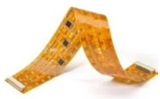
Fig. 1 [3] shows a electronic unit obtained by mounting an ECs on a FPCB. The flexibility of the PCB base allows it to be bent in the desired directions, shaping the cavity in which it is to be installed.
FPCBs can also be used solely for electrical connections, i.e., without installed ECs. Such FPCBs, as a special case, are also called flexible printed cable and are shown in Fig. 2 [3]. However, they, too, and to an even greater extent due to the absence of ECs and the consequent risk of bending affecting the integrity of contact connections, possess the properties of flexibility and impart a three-dimensional structure.
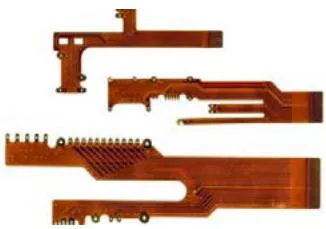
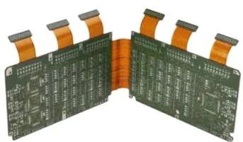
Figure 3 [17] shows a rigid-flexible printed circuit board assembly formed by rigid and flexible printed circuit boards with installed ECs. This example provides flexibility in the relative positioning of the RPCBs, as well as flexibility in external connection of the assembly to other devices.
One of the design and technological solutions for creating a RFPCB is presented in the diagram in Fig. 4 [7].
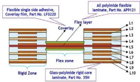
RFPCB consists of two rigid zones and one flex zone connecting the rigid zones. Common to all zones is the flex layer, an all polyimide flexible laminate. The flexible zone also includes two conductive layers and flexible cover layers (coverlay), which are flexible single side adhesive, overlay films on the outer layers. The rigid zones, in addition to the common flexible zone, consist of conductive layers L2 – L9 and outer layers L1, L10 of glass-polyimide rigid core laminate.
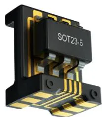
Fig. 5 [10] shows a 3D-MID mechatronic unit demonstrating the adaptation of electrical connections and installed ECs to the complex three-dimensional shape of a mechanical part.
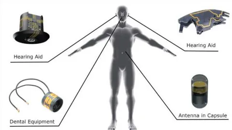
One of the most attractive industries where the efficiency of using 3D-MID technologies is very high is medical technology. Fig. 6 [10] demonstrates some of these devices: elements of a hearing aid, dental equipment, and an antenna in a capsule.
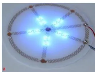

a - flat form before thermoforming;
b - 3D shape after thermoforming
Figure 7: Stages of manufacturing a lamp
The literature review materials and the preceding illustrations serve as the starting point for solving the previously stated problems: creating a cost-effective method for designing 3D printed circuit boards and devices, and a method that will assist electronic equipment designers in selecting optimal DTS for TDPWs.
The solution to the first problem is based on the assertion that RPCBs are the most widely used in production, attractive to electronic equipment designers, reliable, with a variety of design options, and therefore cost-effective. However, they do not fully possess the properties of TDPWs. Further research is devoted to imparting such properties.
The solution to the second problem is determined by the difficulties in formalizing the properties and quality indicators of the considered types of 3D printed connections and, accordingly, the possibility of using purely mathematical optimization methods. For this reason, it is proposed to use a heuristic method and passive game theory, adapted for solving design problems in [18] and [19], to select the optimal design for printed 3D electrical connections and EC assembly.
A method for creating a rigid-flexible printed circuit board: This design and manufacturing method is intended for creating printed circuit boards and, correspondingly, printed circuit assemblies that have a rigid-flexible three-dimensional structure for the placement and connection of ECs. It is suitable for electronic devices with limited volume and irregular structure to improve the layout characteristics of the equipment through more efficient use of the complex shape of the EE [20, 21].
The main driver for developing the proposed method was the economic component associated with the use of more complex technological processes in modern 3D printed circuit assembly methods compared to RPCB manufacturing technology, and the need to acquire new technological equipment, which in some cases is quite complex and expensive.
The objective of the study was to create a printed circuit board and unit based on a RPCB that fully exhibits the properties of a TDPW, i.e., can accommodate two or more rigid parts and a corresponding number of flexible parts for electrical and mechanical connection of the rigid parts and the creation of a 3D structure without the use of assembly and mounting operations; increase the packaging density in the irregular structure of an electronic device; reduce the cost of manufacturing printed circuit boards and the corresponding printed circuit assemblies and create conditions for maintaining signal integrity.
The proposed method is implemented as follows. Initially, a RPCB is manufactured using known technologies for single-sided, double-sided, multilayer, or other boards, taking into account that the board's contour, both external and internal, must correspond to the 3D printed circuit unit. The flexibility of such a board is ensured by creating grooves on its surface in the bending direction of individual board sections. These grooves are deep enough to convert these sections from rigid to flexible. Subsequent assembly of the ECs is performed in a single process cycle on all rigid sections of the PCB separated by grooves. Bending the PCB sections at specific angles and directions allows for the creation of a 3D rigid-flexible printed circuit unit corresponding to the shape and dimensions of the electronic device where it will be installed.
The essence of the method is explained by the figures. Fig. 8 shows a RPCB with grooves 2.1 – 2.3. This creates flexible sections of the board between rigid sections 1.1 – 1.4, allowing sections 1.2–1.4 to be bent along lines 4.1 – 4.3 at specific angles, creating a three-dimensional rigid-flexible structure. To ensure design flexibility, the groove depth must be such that dimension t is no greater than the combined thickness of the foil conductors and the adhesive used to bond them to the dielectric base of the RPCB.
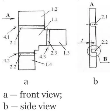
The printed circuit board and the corresponding 3D printed circuit unit are manufactured and used as follows. A flat, rigid printed circuit board (Fig. 8) is manufactured using established technologies. Its contour must match the installation object and subsequent 3D structure formation. To achieve this, grooves 2.1 – 2.3 are created in the board, for example, by milling, at the locations and directions of their subsequent bending 4.1 – 4.3.
In this state, the printed circuit board undergoes electrical installation, i.e., installation of EC 3 and other components, for example for external connection, transforming it into a printed circuit unit (Fig. 9, a).
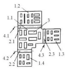
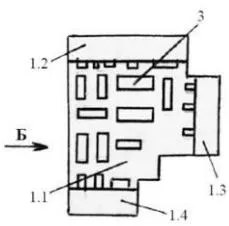
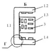
Figure 9: The printed circuit unit after installing ECs By further bending individual sections 1.2 - 1.4 along directions 4.1 - 4.3 at specific angles, the flat printed circuit unit is transformed into a three-dimensional structure, the dimensions and shape of which correspond to the installation object (Fig. 9, b, c).
To strengthen the structure in the flexible sections, polyimide film 6.1, 6.2 can be applied, for example, to foil conductors 5, on both sides and to the walls of grooves 2.1–2.3 (Fig. 10, a).
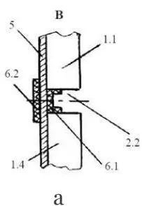
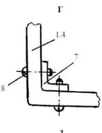
Figure 10: Mechanical reinforcement of parts of a printed circuit board to each other
If additional fixation of individual rigid parts 1.1 - 1.4 is required, fastening elements 7, 8 (Fig. 10, b) can be used.
Thus, a 3D printed circuit unit based on a RFPCB can be installed in electronic devices of various structures, which is especially relevant for devices with complex shapes and limited volume. The proposed method does not claim to be universal, but in some cases it can be used as a more efficient approach.
Method for selecting a three-dimensional printed wiring: As mentioned above, two approaches are proposed as the basis for developing the method: using a heuristic method and the theory of passive games and (Fig. 11).
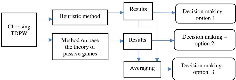
Each of these approaches has its advantages and disadvantages. The first is less expensive and more efficient, but is somewhat subjective. The second, conversely, is more expensive to calculate indicators, but minimizes subjectivity in determining selection results. However, both require the use of weighting factors that take into account the capabilities and conditions of application of various types of TDPW, and their definition is rarely formalized. This also introduces a certain degree of error into the selection results. The decision to use a method is made on a case-by-case basis. Alternatively, both approaches can be used simultaneously and the results averaged.
The implementation of the first approach is based on the heuristic method described in [18]. A prerequisite for the experts' work is their competence in the given area of knowledge, as well as a number of initial data related to the specific development:
A description of the task and challenges of creating an electrical connection design (ECD), determining the feasibility of using varieties of TDPW for this purpose;
Possible layout diagrams of the electronic device being developed;
Questionnaires for evaluating the proposed TDPW types;
A description of the expert voting conditions;
Determination of the ranges of possible expert assessment values in points from the minimum , to the maximum , respectively, for two groups of experts or two rounds of voting.
As initial data for experts to complete the questionnaire, it is proposed to use information with the classification and comparative characteristics of TDPW methods, presented in Table 1. These data can be considered an integral part of the method, as they can be used over a relatively long period of time, updated as new data emerges or as otherwise necessary. They are intended for use by experts when completing questionnaires.
| Indicator | The degree of implementation of TDPW methods | |||
| FPCB | RFPCB | RFPCB on a single base | 3D-MID | |
| 1. PCB type:Single-sided;Double-sided;Multi-layer | YesYesYes | YesYesYes | YesYesYes | YesNoNo |
| 2. ECs:surface-mounted;through-hole;embedded in the board body;heavy and bulky | YesNoNoNo | YesYesYesYes | YesYesYesYes | YesNoNoYes |
| 3. Adaptation to the body shape | High | High | Average | Very high |
| 4. Density of ECs installation | Low | High | High | Low |
| 5. Possibility of creating complex 3D shapes | High | High | Low | Very high |
| 6. Accuracy of installation of ECs relative to the body | High | Average | High | Very high |
| 7. Set of construction materials | Small | Large | Small | Very large |
| 8. Weight ECD | Small | High | High | Very small |
| 9. Heat resistance | High | Low | Low | Low |
| 10. Signal integrity issues | No significant | Significant | Minimal | No significant |
| 11. Difficulty of repair | Increased | High | Low | Very high |
| 12. Problems with testing boards and units | Significant | Significant | Minimal | Significant |
| 13. Potential reduction in durability due to excessive flexing | Significant | Significant | Not significant | No |
| 14. Continuity of the RPCB technology | High | High | Very high | Very low |
| 15. Complexity of technology | Not high | High | Not high | Very high |
| 16. Comparative cost | Average | High | Low | Very high |
The subjective factor of this method is overcome by developing and maintaining information data that classifies and characterizes the set of selected technical solutions inherent to certain DTSs, such as the RFPCB. The influence of the subjective factor is mitigated by the use of various statistical tests: the correlation coefficient, the Fisher test for equality of variances, and the Student's t-test. Automation of the selection process facilitates the practical application of the method. An example of the use of the proposed method is provided in the next section.
The implementation of the second approach involves the use of a number of TDPW indicators that have a mathematical representation [19]:
- The indicator of the specific mean time between failures of a connection – represents the time between failures of one connection, characteristic of a certain type of TDPW
where – failure rate of the i-th connection;
- failure rate of the j-th contact;
n - number of connections in the design TDPW;
d - number of contacts in the design TDPW;
- Indicator of the reduced delay time of information transmission
where – signal delay in the i-th connection of the information transmission path;
- length of the i-th connection;
- Automation factor for electrical connections
where – number of connections performed by automated methods.
In this case, this coefficient should be understood not only as connections on the boards, but also as connections on the boards inside the electronic module.
Additionally, it is proposed to use TDPW-specific indicators:
- Automation coefficient for mounting ECs on boards
where – the number of ECs that are installed using automated methods; – total number of installed ECs;
- Coefficient of the volume of the TDPW design
where – volume occupied by the TDPW design; – volume of the electronic module;
- Coefficient of the weight of the TDPW design
where – weight of the TDPW design;
– weight of the electronic module;
- Signal reflection coefficient in transmission line inhomogeneities
where - reflected signal amplitude; - amplitude of the transmitted signal;
- Mounting space utilization coefficient; characterizes the reduction in volume of the electronic device body where the electronic circuit is placed using one of the TDPW methods, compared to rigid printed wiring
where , – the volume required for the placement of an electronic circuit using, respectively, a TDPW and a two-dimensional rigid printed circuit board;
- Indicator of adaptation of TDPW types to the shape of the body of the ED being developed
where N – the number of body shapes available and suitable for placement electronic circuits; – the number of body shapes possible for the implementation of a specific type of TDPW.
The following body shapes can be used: cube, parallelepiped, cylinder, sphere, hemisphere, cone, truncated cone and others, as well as their combination in one design;
- TDPW flexibility indicator
where – the maximum permissible number of bends in the structure (for example, at an angle of ); – minimum bending radius (for example in mm).
Having calculated the given coefficients and indicators, we can determine the optimal variant of the TDPW the electronic device being developed, using the theory of passive games . An example of the method's use is given in the next section.
IV. EXPERIMENTS
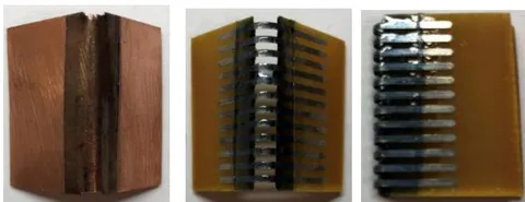
Testing the practical feasibility of the RFPCB manufacturing method: The above-described technological processes for RFPCB manufacturing were experimentally performed to confirm their feasibility. The basis for the experiments were two blanks made of single-sided foil-clad fiberglass, one with a continuous foil layer, and the other with foil tracks.
One of the most critical processes is the production of grooves for flexible sections. High precision machining is required, as mentioned earlier, for example, by milling. The challenge lies in precisely removing the foil or foil traces from the fiberglass laminate, and preferably from the adhesive, without damaging these conductive elements. Chemical etching can replace mechanical machining. However, the fiberglass laminate must be etched to a sufficiently deep depth. A combination of these two methods—preliminary high-speed machining without precision and chemical etching of a small remaining portion of the fiberglass laminate without the risk of damaging the foil conductive traces - can yield good results.
The second issue regarding the production of grooves, i.e., flexible parts, is determining their width. It depends on the bend radius, the thickness of the rigid part of the PCB, the angle of rotation of the rigid parts relative to each other, and other characteristic dimensions of the RFPCB. Let's consider this using the example in Fig. 12, which contains the initial data for the calculation regarding the two most typical cases, taking into account the assumption that the bending radius of the flexible part r is equal to the thickness of the rigid part t.
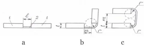
a - a workpiece; b - at a bending angle of ; c - at a bending angle : 1 - rigid part; 2 - flexible part
Figure 12: Determining the groove width on a workpiece
- The bending angle of the rigid parts is . The groove width l is determined using the following relationship
At m = 0, i.e. when the rigid parts are located in close proximity, the minimum groove width is
- For the case of bending rigid parts by
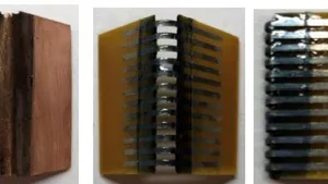
Fig. 13 shows photographs of printed circuit boards with grooves made.
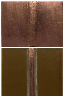
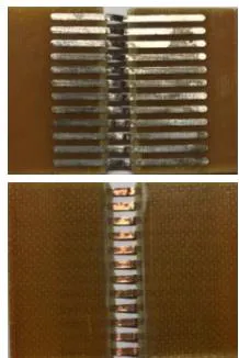
Each version contains two images: the top one is from the foil side, the bottom one is from the fiberglass side and the grooves are made.
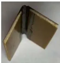
To increase the reliability of the flexible part, it must be made similar to the FPCB, i.e., a polyimide layer must be applied to one or both sides using a polyimide varnish. After this, the flexible part will be identical to the FPCB in its mechanical and electrical characteristics.
Fig. 14 shows photographs of the PCB with polyimide layers applied to both sides.

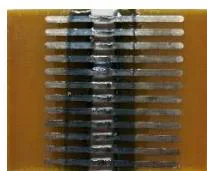

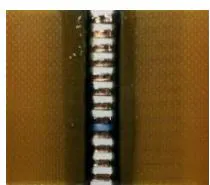
Figure 14: Printed circuit boards that meet the properties of the RFPCB:
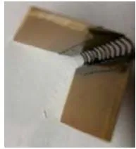
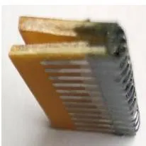
On such RFPCBs it is possible to install ECs and other elements and give them a three-dimensional shape, which is demonstrated in Fig. 15, but only without ECs.
Selecting a three-dimensional printed wiring using a heuristic method: We will examine the use of this method using an example created according to the algorithm (Fig. 1)[18].
1. Initial data for completing the questionnaires:
Select the type of TDPW to create an electronic module to be embedded in a given volume, for example, a medical device, a sketch of which is attached. A schematic diagram of the module and a list of electronic components are also provided. A distinctive feature of the volume allocated for the module is its irregular structure – a combination of a parallelepiped and a truncated cylinder. It is assumed that the printed circuit usit for this electronic module will be manufactured by contract manufacturing, and pre-production preparation with the purchase of new equipment is not necessary. Important factors for selecting the optimal option include manufacturing cost and reliability indicators;
Quantitative data should include module dimensions and dissipated thermal power;
Questionnaire forms;
Voting conditions: two expert groups, each consisting of 5 people;
The range of possible expert assessment scores: from 0 to 10 inclusive for both groups;
A description of the TDPW indicators and their characteristics (Table 1).
- Completion of questionnaires by experts. There should be as many questionnaire forms as there are experts involved, in this case – 10. The questionnaire form and an example of its completion are provided in Table 2. For a more objective assessment of the TDPW options and the assignment of points, we use the indicators and the degree of their implementation (Table 1). Regarding [18], this corresponds to the modified algorithm.
Table 2 Designing High-Dense-Packed Electronic Equipment using Three-Dimensional Printed Wiring
| Indicator | Points awarded for types of TDPW | Weighting factor, | |||
| FPCB | RFPCB | RFPCB on a single base | 3D-MID | ||
| 1. PCB type: | |||||
| - single-sided; | 10 | 10 | 10 | 10 | |
| - double-sided; | 10 | 10 | 10 | 2 | 0,1 |
| - multi-layer | 10 | 10 | 10 | 0 | |
| 2. ECs: | |||||
| - surface-mounted; | 10 | 10 | 10 | 10 | |
| - through-hole; | 0 | 10 | 10 | 0 | |
| - embedded in the board body; | 0 | 10 | 10 | 0 | 0,08 |
| - heavy and bulky | 0 | 10 | 10 | 10 | |
| 3. Adaptation to the body shape | 8 | 6 | 5 | 10 | 0,12 |
| 4. Density of ECs installation | 6 | 10 | 10 | 5 | 0,1 |
| 5. Possibility of creating complex 3D shapes | 8 | 6 | 5 | 10 | 0,11 |
| 6. Accuracy of installation of ECs relative to the body | 8 | 6 | 8 | 10 | 0,04 |
| 7. Set of construction materials | 10 | 8 | 10 | 5 | 0,06 |
| 8. Weight ECD | 10 | 6 | 6 | 10 | 0,03 |
| 9. Heat resistance | 10 | 6 | 6 | 5 | 0,04 |
| 10. Signal integrity issues | 8 | 5 | 10 | 8 | 0,06 |
| 11. Difficulty of repair | 8 | 6 | 10 | 4 | 0,03 |
| 12. Problems with testing boards and units | 5 | 5 | 10 | 8 | 0,02 |
| 13. Potential reduction in durability due to excessive flexing | 6 | 6 | 8 | 10 | 0,03 |
| 14. Continuity of the RPCB technology | 8 | 6 | 10 | 2 | 0,05 |
| 15. Complexity of technology | 10 | 7 | 10 | 4 | 0,05 |
| 16. Comparative cost | 8 | 6 | 10 | 3 | 0,08 |
| 9,6 | 7,2 | 8,4 | 6,4 | ||
The use of weighting factors eliminates the possibility of overcompensation between indicators and improves the reliability of selecting the optimal type TDPW. These factors are assigned by each expert, and the sum of these factors must equal one.
The last row in the table represents the sum of the products of the assigned points by the weighting factor for each installation type and is the expert's final result. All experts in groups X and Y must complete the tables in a similar manner. The resulting expert data is summarized in Table 3 to convolve the indicators (the table format is given in [18]).
Indicators can be characterized by several components. In this example, these are indicators 1 and 2. In this case, the average value of indicator is calculated .
Table 3
| Type of TDPW | |||||||||||||
| 1. FPCB | 9,6 | 8,5 | 9,2 | 7,8 | 7,1 | 42,2 | 6,8 | 9,5 | 8,8 | 7,8 | 8,2 | 41,1 | 83,3 |
| 2. RFPCB | 7,2 | 6,8 | 6,9 | 6,3 | 6,8 | 34,0 | 5,7 | 8,1 | 7,3 | 6,4 | 7,3 | 34,8 | 68,8 |
| 3. RFPCB on a single base | 8,4 | 7,6 | 8,1 | 6,7 | 6,5 | 37,3 | 6,1 | 8,3 | 7,7 | 6,9 | 7,5 | 36,5 | 73,8 |
| 4. 3D-MID | 6,4 | 5,7 | 6,6 | 6,5 | 6,2 | 31,4 | 5,2 | 7,1 | 6,9 | 6,2 | 6,7 | 32,1 | 63,5 |
- Determining the consistency of expert assessments based on the value of the correlation coefficient [18]
where
Based on this, it can be considered that the agreement between the experts' assessments is satisfactory.
- Assessing the equality of dispersion using Fisher's test. We calculate the value of and compare it with the table (table II.6 of appendix [22]). For the degree of freedom and the chosen significance , , which is greater than F, indicating that the experts' opinions are homogeneous.
5. Testing the hypothesis of equality of average values using Student's t-test:
- The Student's t-test is determined
where
The degree of freedom is calculated ;
In table of appendix [22], in the row corresponding to , the t value closest to the calculated value is selected; this is t = 0.265. This corresponds to a value of ;
The significance level is determined ;
The condition is checked: .
This condition is met, thus confirming the hypothesis of equality of average values.
Thus, for the example under consideration, the type of TDPW defined in table 3 can be adopted – this is montage using a FPCB.
If these statistical tests did not satisfy the specified significance levels, then a re-vote would be necessary, changing the composition and/or number of experts in the groups.
Selecting a three-dimensional printed wiring using passive game theory. The initial data for this method are the indicators taken from [19] - (1) - (3) and those proposed in this paper - (4) - (10).
We calculate the values of these indicators and summarize them in Table 4.
Table 4
| Type of TDPW | Values of the Indicators | |||||||||
| (K1) | , c/M (K2) | Ka(Kj) | (K4) | (K5) | (K6) | (K7) | (K8) | (K9) | , 1/MM (K10) | |
| 1. FPCB (Y1) | 0,9 | 0,9 | 0,05 | 0,1 | 0,1 | 0,8 | 0,7 | |||
| 2. RFPCB (Y2) | 0,8 | 0,8 | 0,25 | 0,4 | 0,3 | 0,5 | 0,4 | |||
| 3. RFPCB on a single base (Y3) | 0,8 | 0,9 | 0,2 | 0,3 | 0,1 | 0,5 | 0,4 | |||
| 4. 3D-MID (Y4) | 1,0 | 0,7 | 0,01 | 0,02 | 0,1 | 0,9 | 1,0 | - | ||
To facilitate subsequent processing of the results, the table provides additional designations for the TDPW types and indicator values .
To convolution the partial quality indicators, it is necessary to perform a number of operations related to the following:
Some of them are maximized, i.e., the higher the indicator, the better, while others are minimized, i.e., the lower the indicator value, the better;
The partial indicators are different in physical nature, dimensionless, and, as a rule, differ significantly in magnitude;
The partial indicators have different effects on the integral quality indicator, which is used to determine the optimal TDPW type.
Based on the above, the following steps must be taken:
Divide the matrix (table 4) into two: one with the maximized quality indicators: , , and the other with the minimized indicators: ;
Normalize the quality indicator values using the ratio
where max is the maximum value of the j-th quality indicator, i.e., the maximum value in each column;
- Determine the weighting coefficients using expert analysis and multiply the partial indicators by them.
Let's create game matrices whose rows Yi correspond to the types of TDPW, and columns Kj correspond to the partial quality indicators, the calculated values of which ij (Table 4) are entered into the cells of the matrices: table 5 - with the maximized indicators, and Table 6 - with the minimized indicators.
Table 5
| Type of TDPW | Values of the Indicators | |||||
| 0,9 | 0,9 | 0,8 | 0,7 | |||
| 0,8 | 0,8 | 0,5 | 0,4 | |||
| 0,8 | 0,9 | 0,5 | 0,4 | |||
| 1,0 | 0,7 | 0,9 | 1,0 | - | ||
| max | 1,0 | 0,9 | 0,9 | 1,0 | ||
| 0,2 | 0,15 | 0,15 | 0,25 | 0,15 | 0,1 | |
Table 6
| Type of TDPW | Values of the Indicators | |||
| 0,05 | 0,1 | 0,1 | ||
| 0,25 | 0,4 | 0,3 | ||
| 0,2 | 0,3 | 0,1 | ||
| 0,01 | 0,02 | 0,1 | ||
| max | 0,25 | 0,4 | 0,3 | |
| 0,1 | 0,4 | 0,2 | 0,3 | |
As a result of normalization and multiplication by the weighting coefficient, we obtain normalized weighted matrices: Table 7 – with the indicators that are maximized, and Table 8 – with the indicators that are minimized. Here we also perform the convolution of the indicator values. Table 7
| Type of TDPW | Values of the Indicators | Convolution | |||||
| 0,2 | 0,135 | 0,15 | 0,225 | 0,105 | 0,1 | 0,915 | |
| 0,14 | 0,12 | 0,135 | 0,14 | 0,06 | 0,1 | 0,695 | |
| 0,17 | 0,12 | 0,15 | 0,14 | 0,06 | 0,05 | 0,69 | |
| 0,08 | 0,15 | 0,12 | 0,25 | 0,15 | - | 0,75 | |
Table 8
| Type of TDPW | Values of the Indicators | Convolution | |||
| 0,057 | 0,08 | 0,05 | 0,1 | 0,287 | |
| 0,086 | 0,4 | 0,2 | 0,3 | 0,986 | |
| 0,071 | 0,32 | 0,15 | 0,1 | 0,641 | |
| 0,1 | 0,016 | 0,01 | 0,1 | 0,226 | |
To determine the optimal variant of the TDPW among those considered, we will perform a convolution of the total values of the maximized and minimized values of the quality indicators for each type of TDPW in the form of a private
We obtain the following Y values for the TDPW types: FPCB = 3.188; RFPCB = 0.705; RFPCB (on a single base) = 1.076; 3D-MID = 3.319.
In this case, the optimal solution would be to use 3D-MID technology to create an electronic module using TDPW.
The obtained results cannot be taken as estimates, as the values of the individual indicators were assigned without taking into account the actual initial data and corresponding calculations. The purpose of the provided examples is to demonstrate the practical application of the proposed methods.
V. RESULTS
The result of this work is the development of a design and manufacturing method for rigid-flexible printed circuit boards and methods for selecting a three-dimensional printed wiring using a heuristic approach and passive game theory. These methods, while seemingly completely different in their focus, are in fact united by the common goal of creating an optimal design for electronic modules using TDPWs.
A design for a rigid-flex printed circuit board and some manufacturing process features are proposed and described. The main feature of this board is that it is manufactured on a single base—a rigid PCB—for both the rigid and flexible sections. Its manufacturing processes are essentially the same as those used for traditional RPBs and share significant similarities. Experiments were conducted to fabricate RFPBs on a single base, revealing some of the design and manufacturing features and confirming the feasibility of creating 3D printed circuit design and their industrial production.
A sequence of steps for implementing a heuristic method is presented. TDPW indicators and their characteristics are developed, which serve as initial data for experts selecting the optimal TDPW option. The practical application of the method is demonstrated through an example, which also includes statistical verification of expert data to eliminate subjectivity in their testimony. This example demonstrates the feasibility of its rapid implementation, especially if the processing of expert indicators is automated.
A method for using passive game theory to solve the problem of selecting an TDPW option is presented. A series of formalized indicators, supplemented by indicators from , have been developed for this purpose. The given example of TDPW selection clearly demonstrates its application, which, with appropriate automation, also presents no significant difficulties. However, it should be noted that determining the initial data for calculating the indicators is quite labor-intensive. However, this, in turn, is rewarded with more accurate results, as they are less susceptible to the influence of subjective factors.
If it is necessary to obtain the most reliable results possible, it is recommended to use both methods to solve the same problem, and determine the final result by averaging or other approaches.
VI. DISCUSSION
The results obtained regarding the design and manufacturing method for the single-base RFPCB allow us to discuss its practical application. A study of its characteristics revealed its competitiveness compared to other types of TDPW. This is all against the backdrop of its design simplicity, technological continuity, and the cost-effectiveness of production and manufacturing development. This should be complemented by the originality of the adopted solutions, which were confirmed by the priority and formal review process in the application for the proposed invention .
The choice of technical solutions under conditions of uncertainty and risk plays an important role in new developments, as suboptimal solutions to the assigned problems lead to suboptimal results and, in many cases, to the reworking of the work performed. Therefore, the importance of making the right decisions is undeniable, but, on the other hand, methods for obtaining reliable results and ease of use are needed. There is a considerable amount of theoretical research in this area, but there is a lack of developments with a systematic approach and, consequently, methods that would describe the practical implementation of the selection of design and technological solution in the early stages of design.
In this regard, the research conducted and the results obtained in this paper will, to a certain extent, fill the existing gap and provide developers with a tool for the correct selection of DTS. A distinctive feature of the proposed methods is their applicability in a variety of settings. The heuristic method allows for quick and cost-effective implementation, but is somewhat subjective. The method using passive game theory is largely free of subjective decisions, but requires more effort for optimization. The choice of the appropriate method is left to users, taking into account their specific circumstances. For particularly challenging developments, it is possible to use both methods to solve a specific problem and make a final decision.
VII. CONCLUSIONS
This paper addresses the problem of developing methods for creating printed circuit boards for three-dimensional printed wiring and selecting optimal electrical connection designs for them during the design of EE. The novelty of the obtained results lies in the following:
A design and manufacturing method for creating RFPCB has been further developed. This method utilizes a single blank to produce both rigid and flexible components. This method eliminates the need to manufacture separate rigid-flexible PCB components from different materials and perform assembly operations to connect these components. This improves the productivity and efficiency of RFPCB manufacturing and their associated printed circuit units, enhances their layout characteristics, and eliminates the potential loss of signal integrity when transitioning from a rigid to a flexible component and vice versa.
A heuristic method and a method based on passive game theory for selecting the optimal DTS option for TDPW have been further developed. To this end, a set of metrics for assessing the degree of TDPW implementation has been proposed. A number of formal indicators and coefficients for assessing the types of TDPW have also been developed.
The practical value of the proposed methods lies in their readiness for use, as demonstrated by the production of RFPCB samples and calculation examples.
Prospects for further research. Regarding methods for selecting TDPW types, in order to improve reliability and simplify use, it is advisable to continue research on the following issues:
Detailing TDPW indicators and their characteristics to simplify the work of experts and overcome subjectivity.
Increasing the number of formal indicators and coefficients and developing initial data for their calculation.
Creating software and databases to automate calculations.
Expanding the range of TDPW types and their modifications for consideration for potential use.
ACKNOWLEDGEMENTS
The author expresses gratitude to her wife, Efimenko Nina I. for her support during the writing of this manuscript.
Conflict of Interest
The authors declare no conflict of interest.
Ethical Approval
Not applicable
Data Availability
The datasets used in this study are openly available at [repository link] and the source code is available on GitHub at [GitHub link].
Funding
This work did not receive any external funding.
References
Cite this article
Related Research

Special Issue
Launch a focused special issue to highlight research, emerging trends, and expert insights in your academic field.