


Abstract
Theoretical work corresponding to the hope of extracting, without contradicting EMMY NOETHER theorem, a new energy present everywhere in the universe : The vacuum energy . Cyclic vibrations of a piezoelectric bridge embedded at its two ends are created thanks to the attractive, omnipresent, permanent Casimir force FCA, between two electrodes. This force FCA is controlled by an automatic Coulomb repulsive force FCO which appears , thanks to the closing of a switch n°1 on a third electrode called Coulomb. Then , the resultant force on the piezoelectric bridge , FCO - FCA, straightens the bridge and gives it a kinetic energy, which will be dissipated by the force FCA. The force FCO disappears by the automatic closing of an in series with the ground switch n°2, just after the opening of the switch n°1 The system vibrates, creating at each vibration a peak of usable electrical power.
Explore Digital Article Text
I. DESCRIPTION OF THE SYSTEM
1.1: Introduction
We know that the quantum vacuum, the energy vacuum, the absolutely nothing, does not exist.
This statement has been proven multiple times and noted by:
Lamb's shift (1947) of atomic emission frequencies: https://quantummechanics.ucsd.edu/ph130a/130_notes/node476.html)
By the force of Van der Waals which plays a very important physicochemical role and had an interpretation quantum 1930 [London] when two atoms are coupled to the same fluctuations in vacuum:https://culturesciences.chimie.ens.fr/thematiques/chimie-du-vivant/les-forces-de-van-der-waals-et-le-gecko
By Hawking's radiation theory, predicted in 1974 and observed on September 7, 2016. Article Observation of quantum Hawking radiation and its entanglement in an analogue black hole: https://www.nature.com/articles/nphys3863
By the experimental verification (1958) of the existence of a force equated by Casimir in 1948. This so-called Casimir force was measured for the first time in 1997:
https://arxiv.org/abs/quant-ph/9907076 https://en.wikipedia.org/wiki/Casimir_effect
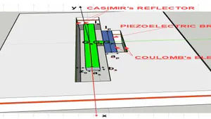
The undisputed interpretation of the above effects involves an energy source coming from some kind of "nothing" or more precisely from the quantum vacuum. So, it is certain that this source of energy causing unmistakable physical manifestations exists. We will therefore choose, for the remainder of this article, a reference frame consisting of the 4-dimensional "Space-time" continuum augmented by those, still unknown, in the "quantum vacuum". In this reference frame we will try to show that the mathematical theorem of the mathematician Emmy Noether is not transgressed. This important mathematical theorem involves in other things the conservation of energy: https://fr.wikiversity.org/wiki/Outils_math%C3%A9matiques_pour_la_physique_(PCSI)/Th%C3%A9or%C3%A8me_d%27Emmy_N%C5%93ther# In this paper we will focus essentially on presenting the detailed energy balance of a MEMS apparently capable of permanently extracting a small amount of energy from the quantum vacuum that can be used in our world. We will try to show that using a piezoelectric bridge deformed by a isotropic, atemporal, attractive, force of Casimir , and straightened by a very ephemeral, repulsive, but more intense force of Coulomb induced by this deformation, an apparent "perpetual movement" of the MEMS device is possible. The schematic of this M.E.M.S. is in figure 4 and 5 In fact, the problem is less to extract energy from the vacuum than to extract it without spending more energy that we cannot hope to recover. The attractive Casimir force is
ref [1],[2],[3]. With the surface of Casimir's electrodes, the reduced Planck constant, and c the speed of light, the interface of Casimir's electrodes. This variation in of , would imply that a larger opposing force is provided to return to the initial position when the interface is smaller.
Coulomb's force can play this role with an energy balance satisfying Emmy Noether's theorem, because -as we shall see- this force will be in : In fact, we know that the fixed charges induced by a Casimir force - in the case of a deformation perpendicular to the polarization of a piezoelectric film are proportional to the Casimir force and are therefore in . We have, with the initial position without any deformation of the piezoelectric film:
ref [4] [5] [6]. In this expression when the electric charge is null. The piezoelectric coefficient is , , , are respectively length and thickness (m) of the piezoelectric bridge. does not depend on the common width bp = bs = bi of the structures (figure 4,5,6). This point is interesting and facilitates the technological realization of these structures since it limits the difficulties of their deep and straight engraving. These fixed electric and ionic charges , inside the piezoelectric bridge, have opposite signs and induce an electric field that attracts from the mass and on the two metallized faces of this bridge, mobile charges of opposite signs.
The mobile charges, for example on face 2 (Fig 4,5), of the faces of the bridge activate the insulating gates of the enriched transistors Thin Film Transistor Metal Oxide Semiconductor T.F.T. M.O.S, N and P in parallel of switch n°1 (Fig 2). It generates on these transistors a gate voltage with the expression (Eq.3). With, Cox the capacity of the grid's transistors (Eq.4) and the permittivity of vacuum, the relative permittivity of silicon oxide, , , the length, width and thickness of the grid of the TFT MOS. The mobile charges of the other face 1 (Fig 4,5) of the bridge supply the sources of the T.F.T. M.O.S. N and P and can circulate to homogenize on a so-called Coulomb electrode, if the threshold voltage of the switch is exceeded. Before closing switch , this Coulomb electrode was grounded by closing switch , consisting of N and P M.O.S. T.F.T's in depletion and in series. (Fig 3). It is important to note that:
1/ The threshold voltage values of these switches are for switch and for switch , and that very slightly above with some tens of millivolts 2/ If the voltage on the insulating gates of the MOS TFTs is above their threshold voltage then: Switch , changes from OFF to ON but conversely switch changes from ON to OFF (Fig 1)
1.2: description of switches n°1 or n°2 and autonomous electronic
1.2.1: switches electronic description
These indispensable switches are made with:
a/ Circuit n°1 (fig 2): with T.F.T. MOS P and MOS N transistors enriched and in parallel: Threshold voltage and
b/ Circuit n° 2 (fig 3): with T.F.T. MOS P and MOS N transistors in depletion and in series: Threshold voltage and
An important point is that the threshold voltage values of these transistors are positioned as Figure 1.
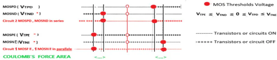
We have: V_{TPE} < V_{TND} < 0 < V_{TPD} < V_{TNE}. For the functioning symmetry |V_{TPE}| can equal |V_{TNE}| and |V_{TPD}| can equal |V_{TND}|. Consequently, as |V_{TND}| < V_{TPE}| and |V_{TPD}| < V_{TNE}|, and with a difference of their values of just some tens of millivolts, circuit switch n^\circ2 commutes, then is open or closed just before circuit switch n^\circ1 switches respectively from closed or open (see figure n^\circ1, 2,3, 4, 5, 6, 18).
1.2.2: Circuit : Switch
Switch n°1 consists -with their threshold or voltage- of enriched N type TFT MOS, in parallel with an enriched P type TFT MOS (fig 1,2), as positioned in fig 2. [11]
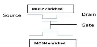
The common gates voltage of these enriched T.F.T. MOS N and P in parallel of switch n°1 (figure 2), are controlled by the free charges appearing on face n°2 of the piezoelectric bridge. The N and P sources of these T.F.T. MOS are connected to face n°1 of the bridge and the drains Coulomb's electrode. (Fig 4,5).
The switch is made with two types of enriched MOSPE or MOSNE transistors in parallel, to avoid the exact nature (holes or electrons) of the mobile electric charges appearing on the metal face of the piezoelectric bridge. Preferably, their threshold voltages are the same in absolute value .
The input of the R.L.C circuit is connected in series between the return Coulomb electrode and the ground, the autonomous electronic n°3 in parallel (figure 4,5). This return Coulomb electrode is itself grounded via switch n°2
1.2.3: Circuit 2: Switches n°2

(see figure 1,3,5). The common gates of these MOS switches are controlled by the free charges appearing on face n°2 of the piezoelectric bridge. (figure 1,4,5). The input of switch n°2 is connected to the Coulomb electrode, and its output to the RLC circuit, then to ground. Preferably, their threshold voltages are the same in absolute value |V_{TND}| = V_{TPD}|. The values of |V_{TND}| \approx |V_{TPD}| are lower but very close (down than 10%) of |V_{TNE}| \approx |V_{TPE}|
1/3: schematic and comportment of the MEMS
Thus, when it is effective (switch n°1 closed), the Coulomb return force is (fig 4,5,6)
We note that is in , with (time dependent) between Casimir electrodes, and distance between Casimir electrodes (without any electric's charges). The schematic of the sensor part of this MEMS is shown in figures (4, 5). The perpetual, isotropic and timeless Casimir force, resulting from quantum vacuum fluctuations, causes the deformation of a microscopic piezoelectric bridge embedded in a silicon wafer.
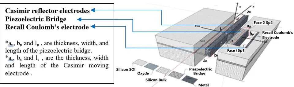
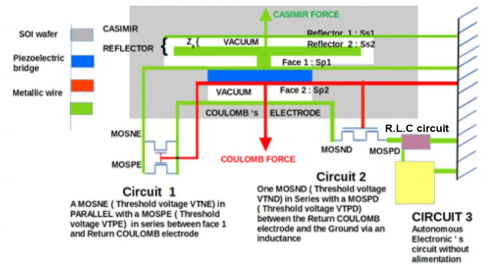
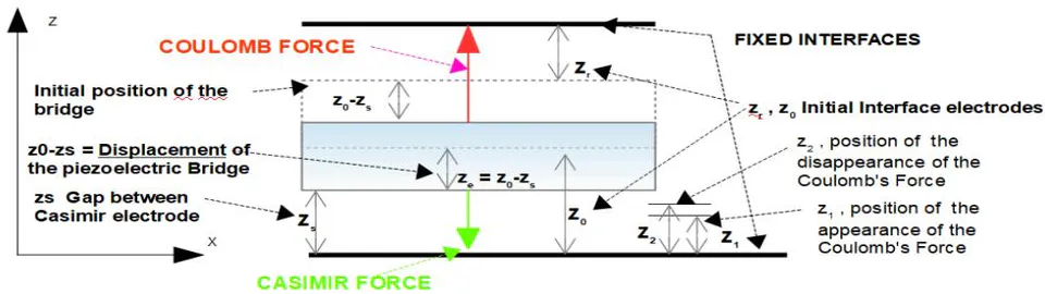
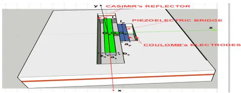
This cycle reproduces itself and the system vibrates (Fig 8,9,10), with the vacuum energy transmitted by the force, as a continuous drive source for the deformation of the piezoelectric bridge and with the self-built Coulomb force , superior and opposed to as the counter-reaction force. At each cycle, the automatic switching of the integrated switches of circuits and (Fig. 1,2,3,4,5,6) distributes differently the mobile electrical charges located on face of the bridge.
Notice that initially, the Coulomb's electrode was grounded by the automatically closing of the switch (Fig 1,3)
II. CALCULATION OF THE BEHAVIOUR OF THE STRUCTURE
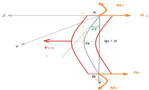
Let us calculate the evolution in time of the deflection of the piezoelectric bridge due to the Casimir's force which is applied between the two electrodes separated by an initial distance (fig 5). We use the theorem of angular momentum for this vibrating structure.(Eq. 6).
With the angular momentum vector of the structure, the inertia matrix of the total structure with respect to the reference (A, x,y,z) and the rotation vector of the piezoelectric bridge with respect to the axis Ay with the low angle of rotation along the y axis of the piezoelectric bridge
We have
Let (Gp, x, y, z), (Gi, x, y, z), (Gs, x, y, z) be the barycentric points respectively of the piezoelectric bridge, of the connecting metal finger and of the metal block constituting the mobile sole of the Casimir reflector. We have (fig 4,5):
The inertia matrix of the bridge, in the frame of reference (Gp, x, y, z) is:
Taking Huygens' theorem into account, this inertia matrix becomes
With the same reasoning we can calculate the inertia matrix of the finger , and the inertia matrix of the reflector in the frame of reference (A, x, y, z),
The total inertia of the structure becomes in the reference (A, x, y, z) is: with A at the edge of the recessed piezoelectric bridge. The angular momentum theorem applied to the whole structure gives:
The structure rotates around the Ay axis, the moments at point A are lp /8 [10], therefore the summation of Moments on the structure relative to the axe .
Any calculation done; we obtain:
with the inertia of the structure relative to the axe Ay.
With , , , respectively the densities of the piezoelectric bridge, the intermediate finger and the mobile electrode of the Casimir reflector. By equation 6, we obtain the differential equation which makes it possible to calculate the interval between the two electrodes of the Casimir reflector as a function of time during the "descent" phase when the Coulomb forces are not present.
This differential equation unfortunately does not have a literal solution, and we programmed it on MATLAB to calculate the duration of this "descent" of the free Casimir electrode. This duration depends on the desired value of the coefficient of proportionality . (See figures chapter 4).
Just at the closing switch , we have with p, a coefficient of proportionality defined by the threshold voltages of the MOS interrupters. Just at the end of "descent" and the start of the charge transfer, the total force exerted becomes: . The "descent" time of the free Casimir electrode will therefore stop when . We can calculate this point where . We know that:
1. The Casimir force is variable in time, but its equation is (Eq. (1)):
The mobile charges transiting from side 1 to the Coulomb electrode through circuit 1 variable also with time (Eq. (2)) are: because they have the same area.
- The Coulomb force (Eq 5), variable over time, acting in opposition to the Casimir force:
- So, the "descent" of the free Casimir electrode stops when the inter electrode interface is such that:
See (Fig 18)
This programmable equation gives the time of the "descent" of the structure submitted to the Casimir force and: a/ depend on the coefficient of proportionality p:
b/ is calculable and will stop when the inter-electrode interface has a value satisfying equation (15).
During all the phases where , or . The total force, variable over time and exerted at the center of the piezoelectric bridge, becomes:
The piezoelectric bridge subjected to this new force rises towards a position where the Coulomb's disappears at the point (fig xx), because the switch 2 closed to ground, via a R.L.C. circuit (fig 4,5). When disappears, the whole moving structure (Casimir reflector electrode + finger + piezoelectric bridge) with an important masse , acquires a kinetic energy with and , Vt = speed of the mobile structures, , respectively the volumic mass and volume of the piezoelectric bridge, finger and Casimir electrode.
Let us calculate an approximation of the duration of this "rise" of the mobile electrode Casimir's reflector + finger + piezoelectric bridge, triggered when . This time is approximated because when the Coulomb force stop (because the closing of the switch to ground at the point between and the initial point , Fig 6), the mobile structure loses its kinetic energy plus its deformation energy with the braking force provided by the Casimir force. We approximate this return time by saying that point of the loss of the Coulomb force occurs at the initial point . In these conditions, to know the time taken by the structure to "go back" to its neutral position, we must solve the following differential equation:
This differential equation (17) has no analytical solution and can only be solved numerically. We programmed it on MATLAB. In these MATLAB simulations we considered that the metal of the electrodes and metal block was oxidized over a thickness allowing to have an interface between Casimir electrodes of 200 A° which modifies the mass and the inertia of the vibrating structure (See chapter 5). It turns out that the choice of aluminium as the metal deposited on these electrodes is preferable given:
The ratio between the thickness of the metal oxide obtained and of the metal attacked by the thermal oxidation (see chapter 6)
Its low density increases and optimizes the vibration frequency of the structure by minimising the inertia of the Casimir reflector and the parallelepiped block that transfers the Casimir force.
The mass of the vibrating structure is then:
. With the density of the metal, , , the geometries of the final metal part of the Casimir electrode sole, the density of the metal oxide, , , the geometries of the oxidized parts around the 6 faces of the metal block, the density of the piezoelectric parallelepiped (see figure 4,5):
III. SIMULATION OF DEVICES WITH DIFFERENT PIEZOELECTRIC BRIDGE
We present below the results of the MATLAB simulations carried out by numerically calculating the differential equations (11) and (13). These numerical calculations give the vibration frequency of the structure which, as we will see, vibrates at a frequency lower than its first resonant frequency (IV). This vibration frequency depends on the characteristics of the structure (Nature of material, geometric dimensions, coefficient of proportionality ). With its low density of 2.7 g cm and its high oxidation power, the metal chosen for the Casimir reflector block is aluminum.
3.1/PMN-PT piezoelectric materials for the piezoelectric bridge
To increase the density of electric charges at the terminals, piezoelectric material PMN-PT can be used. It can be deposited by RF-magnetron sputtering with a composition, for example: ; with piezoelectric coefficient and a Young's modulus .
With MATLAB simulation, and for an interval between Casimir electrode Angstroms, we obtain the evolution over time of the Casimir and Coulomb forces as well as the ratio of figures 8 to 22 below. For a ratio of 1000, the maximum current I delivered by the vibrating structure, the threshold voltage of the MOSE and the vibration frequency of the structure are respectively: , Vt = 3.2 V and 957000 Hertz
3.1.1/Evolution of the Casimir interface as a function of time during two periods: PMN-PT
The ratio = 10000 induces a period of s and a rise time of s with a deflection of the bridge of . The structure vibrates at 259.7 kHz. Due to inertia, at the rise sequence, the structure exceeds the initial by (Fig 28).
{"image_source":{"path":"images/34cc99fb0158e914f496e28bdcbcde2238c677facb18606c63274a96243c5478.jpg"},"content":"","chart_caption":[{"type":"text","content":"Figure 8: Axes, Forces, Casimir's Electrodes"}],"chart_footnote":[]}
A ratio induces a period of s and a rise time of s with a deflection of the bridge of . The structure vibrates at 337.8 kHz: (fig 29).
For this ratio of 1000 we notice a vibration amplitude of , a period of s, with the faster rise of the mobile electrode producing a slight rebound of 5A, because of the inertia of the structure.
{"image_source":{"path":"images/bb10b872933e4f5c65de489abb681fb8ac935d086ca31c317502cf32fb6709f5.jpg"},"content":"","chart_caption":[{"type":"text","content":"Figure 9: plot of the evolution of the Casimir inter-electrode interval as a function of time over two periods and Fco/Fca Ratio = 1000: Casimir inter-electrode interface = 200 A°"}],"chart_footnote":[]} For the ratio (figure 30) a vibration amplitude of just and a period of is obtained. This low deformation of the PMN-PT piezoelectric bridge is mainly due to the extremely high piezoelectric coefficient of 1450 (pC/N) of PMN-PT compared to 120 (pC/N) for PZT. We observe the weak overshoot of the initial interface.
{"image_source":{"path":"images/9b76533ac3bb87b998075a59575f414786b60441e837eda4cc28b73d893233ef.jpg"},"content":"","chart_caption":[{"type":"text","content":"Figure 10: Plot of the evolution of the Casimir inter-electrode interval as a function of time over two periods and a Ratio Fco/Fca = 2. Casimir inter-electrode interface = 200 A"}],"chart_footnote":[]}
3-1-2/Evolution of the forces of Casimir and Coulomb: PMN-PT
We obtain:
1/ The evolution of the Casimir and Coulomb forces as a function a/of the inter-electrode interface (figure 11) and
b/ over time (figure 12)
2/ The / ratio as a function of time for an entire period (figures 13).
{"image_source":{"path":"images/7bb0f835fda2256df7f3890449e6c85dfafcf358a3aee6347e8cf8f501d9d52f.jpg"},"content":"","chart_caption":[],"chart_footnote":[]} {"image_source":{"path":"images/b99d4b4b6b38b6cdf31d98b4b111cbc93de3dca0d9fb36c8661b53f2046f74c5.jpg"},"content":"","chart_caption":[{"type":"text","content":"Figure 12: Materials = PMN-PT: Coulomb and Casimir force as a function of time. Start interface = 200A°"}],"chart_footnote":[{"type":"text","content":"Figure 11: Materials = PMN-PT: Coulomb and Casimir force as a function of the inter-electrode interface. Start interface = 200A°"}]}
It is observed (Fig. 13) that the Coulomb return force is less important for an initial inter-electrode gap than for .
{"image_source":{"path":"images/419767f825ebcaa0037dfe246e9a46bfbfb923793f4b40b8a7668460c50a7af3.jpg"},"content":"","chart_caption":[{"type":"text","content":"PIEZOELECTRIC MATERIAL = PMN-PT\nRatio FCO/ FCA in fonction of time in the cycle"},{"type":"text","content":"Figure 13: Materials = PMN-PT: Coulomb force for "},{"type":"equation_inline","content":"z_{r} = 200 \, A^{\circ}"},{"type":"text","content":" (Blue) and "},{"type":"equation_inline","content":"z_{r} = 400 \, A^{\circ}"},{"type":"text","content":" (Red) and Casimir force (Yellow, "},{"type":"equation_inline","content":"z_{0} = 200 \, A^{\circ}"},{"type":"text","content":") as a function of the inter-electrode interface Starting interface = 200 A"}],"chart_footnote":[]} {"image_source":{"path":"images/f9e3036f9a02a4fbe779f82405d62c5b30174ca3ce7dcc26b43f25b22853bab8.jpg"},"content":"","chart_caption":[{"type":"text","content":"Figure 14: Materials = PMN-PT: Ratio "},{"type":"equation_inline","content":"p = F_{CO} / F_{CA}"},{"type":"text","content":" as a function of time, during a period of vibration.\nStart interface = 200A°, Maximum ratio chosen = 450"}],"chart_footnote":[]}
The break circuits triggered at time s suddenly induce a rise of the mobile electrode, therefore a sudden decrease in electric charges and grids voltages. We observe the gradual evolution towards the chosen ratio of 450 and then the sudden drop in this ratio as the electrodes regain their initial position (Fig. (34)).
3.1.3/Threshold voltage according to the desired Ratio : PMN-PT {"image_source":{"path":"images/9c45f728f0b906a9277234dbc81a7414d1e5985628358be6b069ee5c7c8653ba.jpg"},"content":"","chart_caption":[{"type":"text","content":"Figure 15: Materials = PMN-PT: Threshold voltage of the Enriched or Depleted MOS according to the "},{"type":"equation_inline","content":"F_{CO} / F_{CA}"},{"type":"text","content":" Ratio. Start interface = 200A°"}],"chart_footnote":[]}
It can be seen (Fig. 15) that we must increase the threshold voltage of the TFT MOS of switch n°1 up to 3.5V if we desire to obtain a ratio FCO/FCA of 1000.
.1.4/Vibration frequency as a function of the ratio and peak current as a function of the initial Casimir interval chosen: PMN-PT.
Note (fig 16), that for an initial interface , and for a ratio , the maximum vibration frequency of the structure is 3.50 MHz. It falls to 750 kHz for a ratio of 1000. These frequencies are still lower than the first resonance of the structure, which is of the order of 7.94 Megahertz. This vibration frequency of the Casimir structure approaches that of the first resonance for weaker interfaces below 200 .
For a ratio , the maximum current delivered by the structure falls as a function of an increase in the initial Casimir interval (Fig 17).
It seems that the piezoelectric material PMN-PT coupled with a conductor like aluminium is an interesting couple for our vacuum energy extraction structure.
{"image_source":{"path":"images/a1659e26b6b0f14c77a96e325584d8abd1f092e330db66ba095f638e775e16ae.jpg"},"content":"","chart_caption":[],"chart_footnote":[]} {"image_source":{"path":"images/660bb750004e12e9dcb6c1535538cacda14e009308ccdb64d854172a6cc7df8d.jpg"},"content":"","chart_caption":[{"type":"text","content":"Figure 16: Materials = PMN-PT: Vibration frequency as a function of the "},{"type":"equation_inline","content":"F_{CO} / F_{CA}"},{"type":"text","content":" Ratio. tart interface = 200A° Start interface = 200A°"},{"type":"text","content":"Figure 17: Materials = PMN-PT: Current peak across the "},{"type":"equation_inline","content":"2 \cdot 10^{-4}"},{"type":"text","content":" H inductance as a function of the starting interval between Casimir electrodes. Start interface = "},{"type":"equation_inline","content":"200A^{\circ}"}],"chart_footnote":[]}
IV. MEMS ENERGY BALANCE
In this part, we will try to make a detailed and exhaustive assessment of the behavior of the MEMS during one vibration. Firstly, we will focus on the first half of this vibration, which we will call the "go" phase, so from the initial position to the position where the switch commutes from OPEN to CLOSE. Secondly, we will focus on the second half of the vibration, which is to say the "return" phase, so from the position z1 to zo passing throw the position z2 where the switch commute from OPEN to CLOSE and put the Coulomb's electrode to the ground canceling the force. Let us recall that the piezoelectric bridge is perfectly elastic, which implies, as with any elastic structure, that the energy expended by a mechanical deformation of the positions from o to 1 is integrally restored when returning. The conditions of use of the piezoelectric bridge (vibrations amplitude) are in the purely elastic domain and we never enter in the domain of plasticity.
In the following we propose to put into equations the energy balance of «go» then in "return "steps.
- < VT < VT , and VT < VT < o and F / F < p. With p the chosen amplification F / F . We note V = abs (VT or VT ) and V = abs (VT or VT ), and call V the voltage due to the mobiles charge on the face 2 of the piezoelectric bridge and appearing on the gate of all the TFT MOS transistors. [11]
4/1 MEMS energy balance during the phase "going" from to
At the start, in the beginning conditions of the "go" phase, we have very small deformations applied to the piezoelectric bridge. Consequently, very small electrical charges are present on it, so the electrical voltages on the grid of the enriched and parallel TFT MOS N and P of switch is lower than their threshold voltage . This witch is open and in the OFF position. On the other hand, as , switch consisting of two TFT MOS N and P in series, operating in depletion mode is closed and in the ON position to ground. In these conditions the so-called Coulomb electrode is to the ground, thus eliminating the Coulomb force .
No moving electric charge appears on the return side of the Coulomb electrode, which is connected to ground by switch 2, which is ON, and isolated from the piezoelectric bridge by switch 1, which is OFF. The Casimir force begins to deform the piezoelectric bridge more significantly. Consequently, the mobiles charge on face 1 and 2 of the piezoelectric bridge therefore the voltage on the gates of transistors of switch and increases. This voltage still lower than the threshold voltage , exceeds now of switch which opens and switches OFF.
The structure being assumed to be perfectly elastic and the amplitudes of the vibrations being extremely low, we will see that the mechanical energy losses by an increase of temperature in the device are negligible.
1/ Note also that the mobile parallelepiped metal electrodes of the Casimir electrodes remain parallel to each other and that the mobile metal Casimir electrode does not deform. It simply transmits its movement to the piezoelectric bridge which deforms but therefore does not heat up. (Fig 4,5)
2/ The expulsion of entropy from the vibrating structure of Casimir is transmitted to the piezoelectric bridge. It causes an extremely slight increase in its temperature and expels this heat to the outside. Let us calculate an order of this magnitude . We note the heat transmitted by the vibrations of the piezoelectric bridge. In first approximation, we can use the well-known formula . , with and \Delta T = \text{temperature variation (^{\circ} K)}
However, we know that: Eq. (18) [10] With: fvib= Vibration frequencies of the piezoelectric bridge, mass of this bridge, which is the only one to deform because the Casimir electrodes are simply in translations. We note the maximum deflection of the bridge (Fig 6).
This heat expended at the level of the piezoelectric bridge causes its temperature to increase. As a first approximation we can say: . With: , .
Consequently
For example, for a PMN-PT piezoelectric film: , , , we then obtain: .
The expulsion of entropy from the vibrating Casimir Electrode is negligible.
We note that simply half of this expended heat occurs in the "go", the second part occurs in the "return" phases of the vibration. During a cycle from to , to deform the elastic piezoelectric bridge during the displacement "go" of the vibration, the quantum energy , given by the quantum vacuum, is used for four different energies:
1/ The mechanical energy for the deformation of the elastic bridge:
2/ The energy to create the fixed charges in this piezoelectric structure:
3/ The energy for the simple displacement of the point of application of the Casimir force in the middle of the bridge:
4/ The expulsion of entropy energy, expended in heat due to the friction of the atoms in the half of the vibration of the bridge heat:
We can write that to deform the piezoelectric bridge from the start position to the position :
This quantum vacuum energy is bigger than the simple translation energy WCASIMIR1. The energies and are stored in the deformed piezoelectric bridge as a potential energy.
1/ The translation energy of the Casimir force is:
The energy represents the translation of the Casimir force from to without considering that this force also deforms an elastic and piezoelectric structure from to .
Now, let's calculate the deformation energy of the piezoelectric bridge fixed at both ends. We know that the deformation energy of an elastic system is the energy that accumulates in the solid body during its elastic deformation. Yet, all Material Resistance book says that the deformation energy of an embedded elastic bridge and for a constant force F is: with , the deflection (arrow) acquired by the elastic bridge subjected to the constant force F. In the case of our piezoelectric bride the force F being the Casimir force, varies in , with the distance z.
So, for a differential deflection dz of the bridge under the force we can write:
This energy is stored in the elastic bridge as a potential energy. The position of the mobile Casimir electrode reaches the limit when the grid voltage on switch reaches its threshold voltage . This reached position is unstable because the Casimir force increases with its position. As a result, the mobile Casimir electrode can collapse. But, when the Casimir electrode is in position , the switch switches to ON. The charges present on the metallic face of the piezoelectric bridge must homogenize with the metallic Coulomb electrode, which was previously grounded by the closing of switch . Note that, when switch switches, switch is still open because the voltage of the TFT MOS of switch are in depletion (Fig 1,4,5,6).
The energy stored in the bridge through its deformation is in
At position of the structure, the memorized elastic energy is
We notice that and that the numerical value of is a little smaller than the expression calculated when was constant: .
2/ During the displacement "go" the energy is also used to generate a potential energy accumulated in the capacity of this piezoelectric bridge which follows the equation: with between the two metallic faces of the piezoelectric bridge, with
We notice that , similarly when the structure reaches position , the same memorized elastic energy occurs. To get for position of the bridge, we simply swap for . In these equations, we use , with ,
We know (Eq2) that the creating fixed charges on this piezoelectric structure is . We have the accumulated mobile charges, coming from the mass, on the surface of the metallic film. This part of is stored in the piezoelectric bridge as potential energy and contributes to the usable energy appearing during a cycle.
So, during the phase "going" from to the total energy coming from the vacuum = is used:
1/to deform the piezoelectric bridge ,
2/ to produce the electrical charges as potential energy ,
3/Translate the point of application of the Casimir Force ,
4/ produce a heat of the structure by the entropic transfer .
We have:
Energy produced by vacuum = (Eq 26) and are potential energies that will be used when the elastic bridge returns to its equilibrium position, that is to say without deformation.
4/2: MEMS energy balance during the "return" phase from to , switch ON, Switch OFF: o < abs ( ) < < =abs ( ). and Ratio = p: (Fig 1)
Figure 15 page 10 above, shows the ratio obtained by the choice - defined during the technological realization of the MEMS- of the threshold voltage of switch .
Now, the voltage on the grids of switch exceeds its threshold voltage and switch commute ON. The switch is till OFF, so the Coulomb's electrode is opened. The free charges , stored on the metal electrodes of face 1 (Fig 1,4,5), passing through one of the MOSE transistors, are uniformly distributed on the Coulomb metal electrode of the surface for example .
If , this metallic Coulomb's electrode therefore has approximately a mobile charge . This homogenization is obligatory because there is no electric field in a perfect metallic conductor. The free charges , stored on face 2 and on all the isolated grids TFT MOS don't move. So, the grid's electrodes and return electrode have opposite free charges. (Fig 4,5,15). A Coulomb force then appears between these two electrodes during the very short time when switch no. 2 is still open, isolating the Coulomb electrode from the ground. The resulting force is now applied to the piezoelectric bridge. This force , is opposite to the force or null. In presence of this force the deformations of the bridge and its electrical charges, so the grid's voltage are necessarily reduced. Since the threshold voltage of switch is lower but very close to (we choose mV), the time duration during which this Coulomb force is exerted is very small (a few nanoseconds).
Very quickly, the switch commutes from OFF to ON, grounding the Coulomb electrode via an R.L.C. circuit, (Fig 23). The Coulomb force vanishes quickly after its appearance at position . The values of and impose that is very close to . So, the energy expanded by the Coulomb force remains low, even if this force is several times that of Casimir in intensity.
The time of existence of is of the order of a few tens of nanoseconds (fig 1,5). The position of appearance of this force is such that and is numerically calculated by MATLAB(fig. 18).
We note that the position depends on the values of the interface's of Casimir's electrodes and of Coulomb's electrodes .
{"image_source":{"path":"images/a489217d0963b1467d852a0c71d2c6835a9b9c19aa7f1c5abae8e0f91dbbc187.jpg"},"content":"","chart_caption":[{"type":"text","content":"Fig. 18: Position of the mobile Casimir electrode "},{"type":"equation_inline","content":"z_{1}"},{"type":"text","content":" where the Coulomb force occurs: "},{"type":"equation_inline","content":"z_{r} = z_{0} = 200A^{0}"},{"type":"text","content":", ls = 500 "},{"type":"equation_inline","content":"\mu"},{"type":"text","content":" m, bs = 20 "},{"type":"equation_inline","content":"\mu"},{"type":"text","content":" m, lp = 50 "},{"type":"equation_inline","content":"\mu"},{"type":"text","content":" m, bp = 20 "},{"type":"equation_inline","content":"\mu"},{"type":"text","content":" m, ap = 10 "},{"type":"equation_inline","content":"\mu"},{"type":"text","content":" m"}],"chart_footnote":[]}
The force is now applied to the mobile structure. This resulting force is at least zero or has a greater intensity than the Casimir force . It contributes with the energy stored in the elastic bridge to straighten the structure and to give it kinetic energy. This force exists as long as switch has not switched to ground, canceling its existence by the dispersion of charges on the Coulomb electrode. We describe below the energy dispensed in the cycle of the piezoelectric bridge positions. We hope to show that a usable energy is possible and not due to any electrical energy applied but by the dissipation of the mobile electric charges to the mass throw the switch and an R.L.C. circuit. (Fig 21)
There are two phases for this return to from to (returning phase):
From to where the Coulomb's force exist and contribute to straighten the elastic structure and to give it kinetic energy,
From to where this acquired kinetic energy, and the remaining energy still stored in the structure which will be dissipated by the energy spent by the Casimir force.
4.2.1 Calculation of energies between and .
As soon as switch has switched to homogenize the electric charges between face 1 of the bridge and the Coulomb electrode, the resulting force straightens this bridge and the electric charges drop. The electric voltage on the grids falls below the threshold voltage of this switch which commutes again very quickly. The energy is write:
This energy exists only between the very close positions and . The literal formulation of energy is possible but its expression is not convenient because it is too complex. We prefer to calculate by MATLAB its numerical value between the value and .
The position of commutation of switch is deduced from the chosen threshold value of switch . We note that we can minimize the value of the energy spent by , by choosing a value of the threshold voltage close but slightly lower than of switch . For example (V).
We use MATLAB to find position of commutation of circuit 2 to cancel the Coulomb's Force , see (Eq 22) and figure 18. We have, at position z2 of the bridge, the electric charge in the TFT MOS.
{"image_source":{"path":"images/606fad9874bcaf8a1b35fd3388836a5ad1a8a849862b72458c7eb513877bf731.jpg"},"content":"","chart_caption":[{"type":"text","content":"Fig 19: Energy of translation of Casimir Force and energy of Coulombs 'Force between its apparition in the position "},{"type":"equation_inline","content":"z_1"},{"type":"text","content":" and its disappearance in position "},{"type":"equation_inline","content":"z"}],"chart_footnote":[]}
We present in figure 21 the curve representing the translation energy of the Casimir force as well as the Coulomb's force the time when the structure is between the positions z and z, which represents a few nanoseconds. We can calculate the energy spent in the first part of return of the structure (from to ) Fig 6, by simply calculating the kinetic energy acquired by the structure when it reaches the position upon its return.
We know that the variation of the kinetic energy is equal to the sum of all the energies supplied or spent on the moving structure. Thus, as we know the numerical value of all these participants in the variation of this kinetic energy , we can write equation Eq.25 which allows us to calculate because all the terms of this equation are known.
and fig 20. All the terms of the equation are known, so we now know the kinetic energy acquired by all the mobile systems in and know when the Coulomb force disappears. All calculations done, we obtain: . We know now the kinetic energy acquired in and know when the Coulomb force disappears.
The structure must now spend this energy which gives it inertia. The braking energy provided by the Casimir force will cancel this kinetic inertia plus that stored in the elastic energy. Let us calculate the final ascent position of the mobile structure. It has an inertia provided by the kinetic energy , a stored elastic energy but is slowed down by the energy provided by the Casimir force.
We can write
We deduce of this equation that the final position zf of the bridge is
We can see in Figure 22 that depending on the acquired inertia, which depends on the energy provided by the Coulomb force, zf can slightly exceed its initial position. We will use this property at the end of this article in order to increase usable energy.
{"image_source":{"path":"images/0d4a63fd5452c3c1338061c27b736e45f45278cd1eb4ff4389fb42516e1adf56.jpg"},"content":"","chart_caption":[{"type":"text","content":"Fig 20: Positions of: 1/ The final rise "},{"type":"equation_inline","content":"z_{f}"},{"type":"text","content":" of the structure, 2/ of the point "},{"type":"equation_inline","content":"z_{2}"},{"type":"text","content":" of disappearance of the Coulomb force depending on the threshold voltage "},{"type":"equation_inline","content":"V_{T2}"},{"type":"text","content":" of switch "},{"type":"equation_inline","content":"n^{\circ}2"},{"type":"text","content":", 3/ of the point "},{"type":"equation_inline","content":"z_{1}"},{"type":"text","content":" of appearance of the Coulomb force depending on the threshold voltage "},{"type":"equation_inline","content":"V_{T1}"},{"type":"text","content":" chosen for switch "},{"type":"equation_inline","content":"n^{\circ}1"}],"chart_footnote":[]}
It is easy to calculate the damping energy that appears between the intermediate position and the final position .
As, at position the switch 2 commutes to ON and puts the Coulomb electrode to ground through the RLC circuit below (Fig 21). The electrical charges present on the Coulombs electrode flow towards the ground, creating a current and a power which remains to be evaluated.
\begin{array}{c} \text { GROUND } \\C _ {\text { Piezo }} \\\text { SWITCH n^2 } \\\text { Electric Charge } Q _ {F} = \frac {d _ {3 1} l _ {P}}{a _ {P}} F _ {C A} \quad \text { Uc } \\\text { I } \quad \text { UL } \quad \text { UR } \\\text { L } \quad \text { R } \\\text { VTI } \end{array}Fig 21: RLC circuit to power the autonomous electronics for converting power peaks into direct voltage. We now evaluate this usable current flowing to ground. We put in the circuit an adjustment capacitance C in series with . We call the equivalent capacity of the two capacities in series. When the switch n°2 commutes, we have the equation (fig 21), with , and . With R a resistance, L an inductance and C a capacity. After rearranging we have the following equation Eq 33.
This differential equation has solutions that depend on the value of its determinant. We choose the values of R, L, C in such a way that the determinant of this equation is positive or vanishes. So, if the solutionis: and then we have . Considering the initial conditions, we obtain:
The peak of current is given when so at the time
Replacing t by in the equation 34 and 35 we obtain the expression for the maximum of the voltage is and of the maximum current ;
{"image_source":{"path":"images/1040de1a776ea1452eaf7ca6c20ea9fccba587acc4400c89782931676c7cb9c4.jpg"},"content":"","chart_caption":[],"chart_footnote":[]} {"image_source":{"path":"images/97fbd2457f3443ca1faa4d96330e37b70886b1f1cf397d6b43dd7f820ed8b44f.jpg"},"content":"","chart_caption":[{"type":"text","content":"Fig 23: The electric current flowing through the capacitance C in series with the capacitance of the Coulomb electrode"},{"type":"text","content":"Fig 23: The electric current flowing through the capacitance C in series with the capacitance of the Coulomb electrode"}],"chart_footnote":[]}
{"image_source":{"path":"images/633f558ce6a49a225ce74b2ef3369f571f0fcefd8b8d5463d1b62814f49d960a.jpg"},"content":"","chart_caption":[{"type":"text","content":"Fig 24: Electrical power of the signal to power the autonomous electronics"}],"chart_footnote":[]}
We note on Fig 23 and 24 that the maximum (s) for the peak current is different than those s for the peak power P(t). The peak power of 1.93 mW is sufficient to power the autonomous electronics of fig 30,31 and obtain a useful voltage of several volts in a few milliseconds. The period of a vibration being (fig 10) of 0.2 s for an of simply 2, the average power over a period is then approximately .
We deduce that the power provided by the system in 1 second is of the order of W.
Knowing the electrical power P(time) we can numerically evaluate this finale and usable energy, by MATLAB. We obtain in fig 25.
The energy balance is completed for the "return" phase to its initial position of the structure.
{"image_source":{"path":"images/6cb35ede845915955d0b4176aef844ce42f8a50f2c7e2eca300c92ea1ccf563c.jpg"},"content":"","chart_caption":[{"type":"text","content":"Fig 25: Balance of the energies of the "go" and "return" phases for the proposed MEMS which seems to be able to "extract energy from the quantum vacuum.""}],"chart_footnote":[]} With Figure 25, we can make the energy balance of the energies provided by the quantum vacuum in the "going" and "returning" phases. The constant energy provided by the quantum vacuum ocean in the "go" phase simply changes its nature and subdivides into other energies in the "return" phase of vibrations. One of these energies in this "return" phase can be used by creating a little electrical energy. We note that the energy necessary for the perpetual maintenance of these vibrations is constantly provided by the isotropic and timeless energy of the quantum vacuum and that it is possible to extract from this gigantic ocean of energy of "nothing" a small electrical and exploitable energy. Whatever the amplification factor, we note that is always slightly lower than , thanks to the choice of
We observed that in the referential of our 4 dimensions Space-Time plus the Quantic Vacuum, the energy is conserved which is consistent with Noether's theorem. This very important theorem of 1905 explains why, as Monsieur de Lavoisier said, "Nothing is created, nothing is lost, everything is transformed."
Remember that energy is defined as the "physical quantity that is conserved during any transformation of an isolated system. However, the system constituted by simply the MEMS device in space is not an isolated system while the system constituted by the MEMS device plus the space plus the energy vacuum seems an isolated system. The part of the MEMS energy sensor vibrates at frequencies depending on the size of the structure and operating conditions, but with an amplitude of just a few Angstroms. These vibrations aren't perpetual motion; they can be continuously powered by vacuum energy from the Casimir force.
The following diagram summarizes the operation of this presented MEMS (Fig 26 and Fig 27)
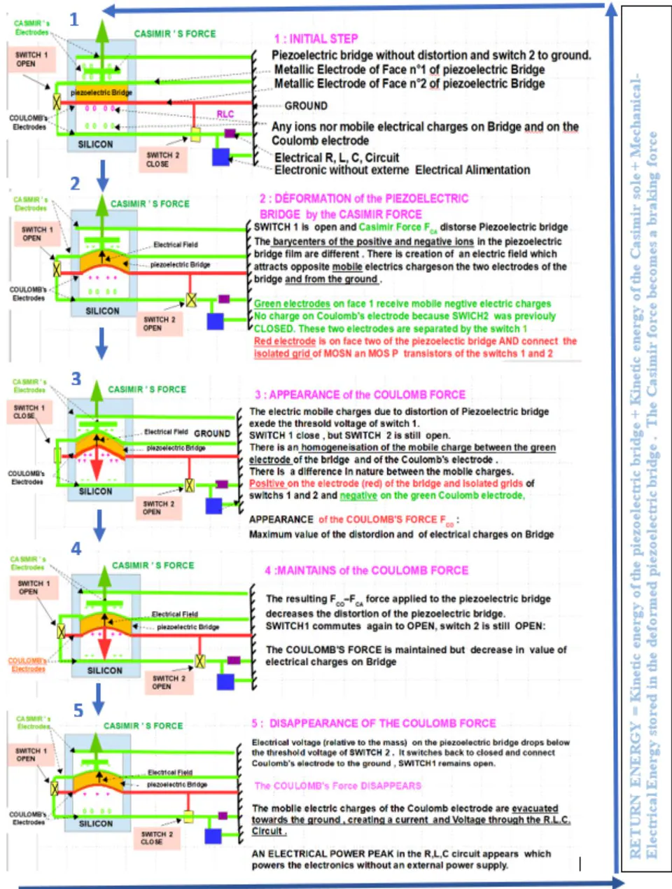
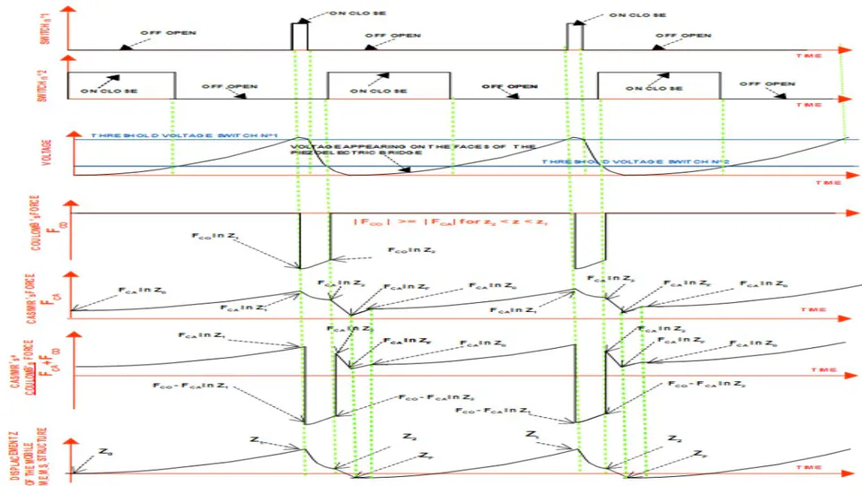
We notice in the previous pages that the piezoelectric bridge could reach a position which exceeds its initial position . We can take advantage of this observation by modifying the moving part of this MEMS to provide the RLC circuit with the two signs of current peak and voltage emitted by the sensor. This modification should increase the continuous electrical voltage on the capacitive output of the autonomous electronic circuit whose role is to transform the signals from the quantum vacuum energy sensor(fig 28)
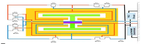
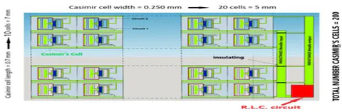
In order to obtain a current peak greater in intensity, the Casimir cells can be positioned in a series and parallel network at the 2 terminals of a single and as described RLC circuit for example, 20 Casimir cells can be placed in parallel and 10 in series, (Figure 29). Important increase in current intensity, time duration of the peak, as of the voltage peak. This work on the energy balance of a M.E.M.S., which appears to be able to extract energy from a new, totally unexploited source, was carried out completely alone and without the help of any organization, by an old retiree. It seems that - unless there is always a possible error - the fundamental theorem of EMMY NOETHER from 1905 is not contradicted. In the event of a theoretical confirmation by specialists, the supreme and definitive judgement will be the realization of a prototype, and I will be happy to participate in this development.
V. AUTONOMOUS ELECTRONICS TO TRANSFORM THE CYCLIC POWER PEAKS FROM THE R.L.C CIRCUIT
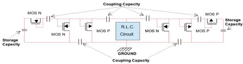
The circuit of the figure 30 is an autonomous device operating without any electrical power source. It rectifies and accumulates the repetitive peak power delivered to the terminals of the RLC circuit in the figure 4 and 5 and transforms them into a usable direct voltage source.
The impedance of the output of this autonomous circuit must be important.
We note the extreme weakness of the electrical power required at the start of the conversion of the power peaks (60 nW) and at the end (2 pW). This transformation requires 4
The circuit of the figure 30 is an autonomous device operating without any electrical power source. It rectifies and accumulates the repetitive peak power delivered to the terminals of the RLC circuit in the figure 4 and 5 and transforms them into a usable direct voltage source. The impedance of the output of this autonomous circuit must be important.
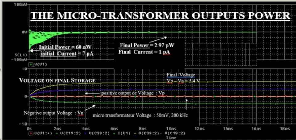
Table 1: Output Continuous voltage, with current and power consumed by the autonomous electronic in function of two input cyclic voltage parametrized with the number of stages CHARACTERISTICS OF OUTPUT VOLTAGES (V), POWERS (nW) CURRENTS (nA) AS A FUNCTION OF THE NUMBER OF STAGES INPUT SIGNAL FREQUENCY = 150 kHz OUTPUT VOLTAGE MEASUREMENT FOR t = 50 ms The interesting points for the presented electronics' device are:
| number of stages | Vg=50mV | Vg=100mV | ||||||||
| Output Voltage | Current (nA) start end | Power (nW) start end | Output Voltage | Current (nA) start end | Power (nW) start end | |||||
| 2*3 | 550mV | 300nA | 26nA | 15nW | 1.3nW | 1.1v | 800nA | 46nA | 75nW | 5nW |
| 2*6 | 1 | 300nA | 29nA | 13nW | 1.3nW | 2V | 700nA | 67nA | 60nW | 6.5nW |
| 2*14 | 2.2v | 300nA | 40nA | 14nW | 2.6nW | 4.5v | 700nA | 50nA | 65nW | 4.8nW |
| 2*21 | 2.8v | 250nA | 38nA | 13nW | 860pw | 6v | 600nA | 80nA | 60nW | 2.7nW |
| 2*30 | 3.3 | 250nA | 43nA | 12nW | 1.2nW | 6.5V | 750nA | 85nA | 61nW | 4nW |
| 2*39 | 3.5v | 250nA | 45nA | 12nW | 900pW | 7.5V | 750nA | 95nA | 64nW | 3.5nW |
| 2*48 | 3.6v | 250nA | 46nA | 12nW | 1nW | 7.6V | 750nA | 100nA | 60nW | 4.2nW |
| 2*60 | 3.8 | 270nA | 47nA | 12nW | 1.1nW | 7.9V | 700nA | 90nA | 65nW | 4.2nW |
| 2*61 | 3.8 | 270nA | 48nA | 12.1nW | 1.3nW | 8V | 700nA | 90nA | 65nW | 42nW |
The low alternative input voltages required to obtain a continuous voltage of several volts at the output
The low power and current consumed by this conversion and amplification circuit on the source which in this case is only R.L.C. circuit, supplied by the current peaks generated by the autonomous vibrations.
3. The rapid time to reach the DC voltage (a few tens of milliseconds)
The technology used to fabricate the TFT (Thin Film Transistors) [11] MOSNE and MOSPE transistors with the lowest possible threshold voltages, is CMOS on intrinsic S.O.I. and each element are isolated from each other on independent islands. This technology, represented in the following figure 54, strongly limits the leakage currents.
We note that the coupling capacities of 20 pF of this electronic, like that of storage of the order of 10 nF, have relatively high values. To minimize the size of these capacitor we propose to use of titanium dioxide as insulator, with a relative permittivity of the order of 100 which is one of the most important for a metal oxide, then the size of the capacity passes to 33 m for a thickness of TiO = 500 A , which is more reasonable.
IV. TECHNOLOGY OF REALIZATION OF THE CURRENT EXTRACTOR DEVICE USING THE FORCES OF CASIMIR IN A VACUUM
For the structures presented above, the space between the two surfaces of the reflectors must be of the order of ,.... which is not technologically feasible by engraving. Yet it seems possible to be able to obtain this parallel space of the order of between Casimir reflectors, not by etching layers but by making them thermally grow. Indeed, the and surfaces of the Casimir reflector must;
Be metallic to conduct the mobile charges
insulating as stipulated by the expression of Casimir's law who established for surfaces without charges.
This should be possible if we grow an insulator in the z direction of the structure, for example or or other oxide metal which is previously deposited and in considering the differences in molar mass between the oxides and the original materials.
For example, silicon has a molar mass of 28 g/mol and silicon dioxide SiO of 60 g/mol. It is well known that when a silicon dioxide SiO grows by one unit, a silicon depth of about 28/60 = 46.6%. This means that the fraction of oxide thickness "below" the initial surface is 46% of the total oxide thickness according to S.M. Sze. [9] The same must happen, for example for thermal growth of alumina. The molecular masses of Alumina and aluminium are M = 102 g/mole and M = 27 g/mole. We obtain an aluminium attack ratio of 27/102 = 26%, which implies that the original surface of this metal has shifted by 26% so that 74% of the alumina has grown out of the initial surface of the aluminiu. As regards the technological manufacture of electronics and structure, it therefore seems preferable:
For electronics to choose Titanium Oxide because of its high relative permittivity allowing to minimize the geometries required for the different capacities.
For the Casimir structure, the choice of aluminium, because its low density increases the resonant frequency of the structure and that 74% of the Alumina Al2O3 is outside the metal, allowing to reduce the interface between Casimir electrodes. A simple calculation shows for example that for aluminium gives:
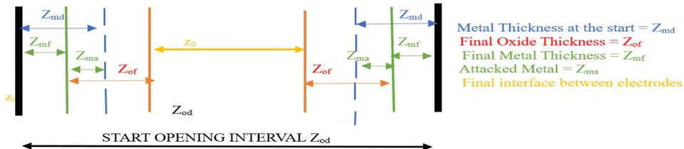
For example, we start from an opening . We deposit a metal layer of aluminium that is etched leaving a width on each side of the reflector. Then an Alumina can grow, the thickness of which is precisely adjusted, simply by considerations of time, temperature, and pressure to increase a necessary thickness to have the desired interface . For example, if , , , then . So, we obtain a Casimir interface of . The final remaining metal thickness will be and will act as a conductor under the aluminium oxide. Obviously, the growth of this metal oxide between the electrodes of the Casimir reflector modifies the composition of the dielectric present between these electrodes, therefore of the mean relative permittivity of the dielectric Let: be the permittivity of vacuum and . the metal oxides one ( in the case of ), the final oxide thickness on one of the electrodes and z the thickness of the vacuum present between electrode, (initially we want ). Then the average permittivity of the dielectric is:
| Métal | Zof, ,Metal Oxide | Z, Vacuum | Zof ,Metal oxide | Métal |
For example, is large compared to therefore in the case of .
We have considered this change in permittivity in the preceding simulations.
VII. STEPS FOR THE REALIZATION OF THE STRUCTURE AND ITS ELECTRONICS
We use an SOI wafer with an intrinsic silicon layer: The realisation start with voltage "doubler" is obtained by using CMOS technology with 8 ion implantations on an SOI wafer to make:
1 /The sources, drains_of the TFT MOSNE, MOSND of the "doubler" and of the Coulomb force trigger circuits and of the grounding
2/The source, drains of the MOSPE, MOSPD of the "doubler" and of the Coulomb force trigger circuits
3/The best adjust the zero-threshold voltage of the MOSNE of the "doubler" circuit
4/The best adjust the zero-threshold voltage of the MOSPE of the "doubler" circuit To define the threshold voltage of the MOSNE of the circuit n°1
7/To define the threshold voltage of the MOSND of the circuit n°2 8/to define the MOSPD threshold voltage of the circuit n°2 This electronic done, we take care of the vibrating structure of CASIMIR 9/engrave the S.O.I. silicon to the oxide to define the location of the Casimir structures (figure 34)

10/ Place and engrave a protective metal film on the rear faces of the S.O.I wafer (figure 35)
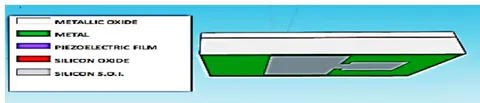
11/Deposit and engrave the piezoelectric layer (figure 36)
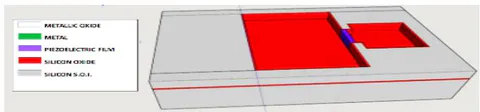
12/ Depose and etch the metal layer of aluminium (figure 37).
{"image_source":{"path":"images/d7c45f7931e1c1d71d37c9b42c8a4ff1cce590b37d9f1405a738b70711b08772.jpg"},"content":"","chart_caption":[{"type":"text","content":"Figure 37: 12/ Metal deposit, Metal engraving etching of the piezoelectric layer"}],"chart_footnote":[]}
13 /Plasma etching on the rear side the silicon of the Bulk and the oxide of the S.O.I wafer protected by the metal film to free the Casimir structure then very finely clean both sides (figure 38) {"image_source":{"path":"images/d95ed71761d4669c0eb0b370ac18354c6c7f26a2f07943d98b0a0c9408ec0be0.jpg"},"content":"","chart_caption":[{"type":"text","content":"Figure 38: 13/ view of the Casimir device on the rear face, engraving on the rear face of the structures."}],"chart_footnote":[]}
14 /Place the structure in a hermetic integrated circuit support box and carry out all the bonding necessary for the structure to function.
15 /Carry out the thermal growth of aluminium oxide with a measurement and control of the circuit under a box. The electronic circuit should generate a signal when the interface between the Casimir electrodes becomes weak enough for the device to vibrate... and then stop the oxidation. (Figure 39)
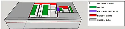
16 /Create a vacuum in the hermetic box
In the case where the 2 metal electrodes of Casimir, adhere to one another, they can be separated by the application of an electrical voltage on the Coulomb's electrodes.
VIII. CONCLUSION
The theoretical results of this project seem sufficiently encouraging to justify the development of prototypes. While theoretical results indicate promising potential, further experimental validation is necessary to confirm the feasibility of harnessing quantum vacuum energy. Future work will focus on developing prototypes and refining the theoretical models to address practical implementation challenges. Of course, if these theoretical predictions are confirmed, it will trigger a scientific, technical and human revolution, because the quantum vacuum could be used as a new source of energy both on Earth and in space with a considerable commercial market. As an inventor who has kept some details confidential, I would like to collaborate in its development after signing a contract with the potential investor In the universe, everything is energy, everything is vibration, from the infinitely small to the infinitely large" Albert Einstein. "A person who has never made mistakes has never tried to innovate." Albert Einstein
Conflict of Interest
The authors declare no conflict of interest.
Ethical Approval
Not applicable
Data Availability
The datasets used in this study are openly available at [repository link] and the source code is available on GitHub at [GitHub link].
Funding
This work did not receive any external funding.
References
Cite this article
Related Research


Special Issue
Launch a focused special issue to highlight research, emerging trends, and expert insights in your academic field.