




IntelliPaper
Abstract
This work reports one-dimensional simulation-based analysis of the performance of thin-film solar cells using Copper Indium Gallium Selenide (CIGS) as the absorber layer. The study focuses on how three key parameters; absorber layer thickness, band gap energy and operating temperature influence the efficiency of solar cells. Simulations were performed using SCAPS-1D under standard illumination conditions (AM1.5G, 1000 W/m²). The absorber layer thickness was varied from 0.8 µm to 2.0 µm, the band gap from 0.8 eV to 1.8 eV and the temperature from 240 K to 360 K. Results show that an optimal combination of these parameters; CIGS thickness of 1.6 µm, band gap of 1.4 eV and operating temperature of 240 Kyields a maximum conversion efficiency of 19.95%. The trends indicate that increasing thickness and band gap improve efficiency up to a limit, beyond which recombination or reduced light absorption lowers performance. Similarly, higher temperatures result in efficiency loss due to increased carrier recombination. These findings provide insight into absorber layer design and optimization for improving the performance of thin-film CIGS solar cells.
Explore Digital Article Text
I. INTRODUCTION
The pursuit of sustainable energy solutions has sparked significant advancements in solar cell technology, with a growing emphasis on enhancing efficiency and performance. As the world continues to grapple with the challenges of climate change and energy sustainability, the development of more efficient solar cells has become a pressing priority[1]. Solar cells, which convert sunlight into electrical energy, are influenced by a complex interplay of critical parameters, including material thickness, operating temperature, and band gap energy. These factors play a crucial role in determining the overall efficiency and functionality of solar cells, making their analysis and optimization vital for the development of next-generation photovoltaic devices[2].
This study utilizes a one-dimensional simulation tool, SCAPS-1D, to analyze the impact of key parameters on solar cell performance[3]. By leveraging the capabilities of this simulation software, we can gain valuable insights into the behavior of solar cells under various operating conditions[4]. The research focuses on modeling and simulating the behavior of solar cells under varying conditions, specifically examining the effects of thickness on photon absorption and charge carrier generation. This involves investigating how different thicknesses of the active layer influence the solar cell's ability to absorb photons and generate charge carriers, which is essential for optimizing device performance[5].
In addition to thickness, temperature variations also play a significant role in determining solar cell efficiency. Changes in temperature can affect the material properties and overall performance of the solar cell, leading to variations in efficiency and output[6]. By simulating the effects of temperature on solar cell performance, one can gain a deeper understanding of the complex relationships between temperature, material properties, and device efficiency. This knowledge can be used to develop more efficient solar cells that can operate effectively across a range of temperatures .
Furthermore, the band gap energy of the solar cell material also has a profound impact on its spectral response to different wavelengths of light. By exploring the relationship between band gap energy and spectral response, we can identify optimal configurations that enhance solar cell performance and efficiency. This involves analyzing how different band gap energies influence the solar cell's ability to absorb and convert different wavelengths of light, which is crucial for optimizing device performance[8].
By investigating these parameters and their interplay, this study aims to identify optimal configurations that enhance solar cell performance and efficiency. The findings are expected to contribute to the understanding of solar cell dynamics and provide valuable insights for designing and fabricating more efficient photovoltaic devices. Ultimately, this research has the potential to inform the development of next-generation solar cells that are more efficient, sustainable and cost-effective.
II. THEORETICAL BACKGROUND
The performance of a solar cell depends on several material and environmental parameters. In thin-film CIGS solar cells, absorber layer thickness, band gap energy, and operating temperature are particularly critical. Understanding the influence of these parameters is essential for optimizing device efficiency and stability.
2.1 Absorber Layer Thickness
The thickness of the absorber layer plays a dual role in solar cell performance. A thicker layer increases the absorption of incident photons, particularly in the longer wavelength range, thereby generating more electron-hole pairs. However, excessive thickness can also lead to increased recombination losses, as charge carriers may not efficiently reach the contacts. Conversely, a very thin layer may suffer from inadequate light absorption. Thus, a balanced thickness is essential for maximizing both light absorption and carrier collection efficiency[9].
2.2 Temperature
Temperature significantly affects the electrical behavior of solar cells. Higher temperatures generally lead to a reduction in open-circuit voltage (Voc) due to band gap narrowing and increased carrier recombination. This results in a decline in overall efficiency. On the other hand, lower temperatures reduce recombination losses, leading to improved Voc and fill factor (FF). However, they may also reduce carrier mobility slightly. Therefore, thermal management is a crucial aspect of solar cell design and installation. A comprehensive understanding of these parameters provides the foundation for simulation-driven optimization using tools like SCAPS-1D .
2.3 Bandgap
The bandgap (eV) determines the range of the solar spectrum that can be effectively absorbed. A wider band gap restricts absorption to higher-energy photons (e.g., blue light), while a narrower band gap allows absorption across a broader range but with lower voltage output. The ideal band gap for single-junction solar cells lies between 1.1 and 1.4 eV, enabling a good compromise between current and voltage output. CIGS offers tunable band gaps within this range, making it a versatile material for optimization [10].
III. METHODOLOGY
This study employs SCAPS-1D (Solar Cell Capacitance Simulator) to simulate a thin-film solar cell structure based on CIGS as the absorber layer. The cell design includes multiple functional layers and contacts, each defined with specific material and electrical parameters. The simulation focuses on analyzing the impact of varying absorber layer thickness, band gap energy, and temperature on solar cell performance.
3.1 Device Structure
The simulated solar cell architecture comprises a multilayer structure, configured from back to front as follows: a molybdenum (Mo) back contact, a copper indium gallium selenide (CIGS) absorber layer, an oxide void CIGS (OVC) passivation layer, a cadmium sulfide (CdS) buffer layer, an intrinsic zinc oxide (i-ZnO) window layer and an aluminum-doped zinc oxide (AZO) front contact. Each layer's properties, including thickness, doping, band gap and mobility, were carefully parameterized based on realistic material values to ensure an accurate representation of the solar cell's performance.
3.2 Simulation Parameters
The SCAPS-1D simulation was performed under standard conditions to ensure accurate and reliable results. The illumination was set to the AM1.5G spectrum at an intensity of , mimicking typical solar radiation . The initial temperature was set to 300 K, and later varied to 240 K and 360 K to investigate the impact of temperature on solar cell performance. The voltage range was set from 0 to 1.0 V to capture the current-voltage characteristics of the solar cell. A total of 100 data points were collected to ensure a detailed and accurate representation of the solar cell's behavior.
The simulator solves fundamental equations, including Poisson's equation and carrier transport equations (continuity and drift-diffusion), to evaluate key performance metrics. These metrics include current-voltage (J-V) and quantum efficiency (QE) curves, providing a comprehensive understanding of the solar cell's behavior and performance[12].
3.3 Layer Configuration and Material Properties
Each layer properties were defined in SCAPS using parameters such as:
Table 1: Material parameters of each layer in the CIGS solar cell
| Layer | CIGS | OVC | CdS | i-ZnO |
| Thickness (μm) | 1.2 | 0.015 | 0.05 | 0.08 |
| Bandgap (eV) | 1.3 | 2.7 | 2.45 | 3.4 |
| Electron Affinity (eV) | 4.5 | 4.2 | 4.45 | 4.55 |
| Doping Type | p-type | n-type | n-type | n-type |
| Doping Density (cm-3) | $1.5 \times 10^{17}$ | $1 \times 10^{18}$ | $1 \times 10^{15}$ | $5 \times 10^{18}$ |
| Electron Mobility (cm2/Vs) | 1000 | 150 | 200 | 50 |
| Hole Mobility (cm2/Vs) | 500 | 30 | 10 | 20 |
Additional parameters such as carrier mobility, thermal velocities and defect densities were also configured based on literature and standard SCAPS data models.
3.4 Contact Properties
The left and right contacts of the solar cell were defined with specific properties to accurately simulate carrier extraction and interfacial behavior. The left contact, made of Molybdenum (Mo), had a work function of 5.54 eV, while the right contact, composed of Aluminum-doped Zinc Oxide (Al:ZnO), had a work function of 4.54 eV. The surface recombination velocities for both contacts were set to cm/s, representing the rate at which charge carriers recombine at the contact interfaces. Contact tunneling was disabled in the simulation. These settings allowed for a realistic representation of the solar cell's behavior .
The simulated solar cell structure, depicted in Figure 1, consists of multiple layers: a Mo back contact, a CIGS absorber layer, an OVC passivation layer, a CdS buffer layer, an i-ZnO window layer, and an Al-doped ZnO front contact. During operation, light enters the solar cell through the top (AZO side), generating charge carriers that are collected through the front and back contacts. This structure and the defined contact properties enable the simulation to accurately model the behavior of the CIGS-based thin-film solar cell[14].
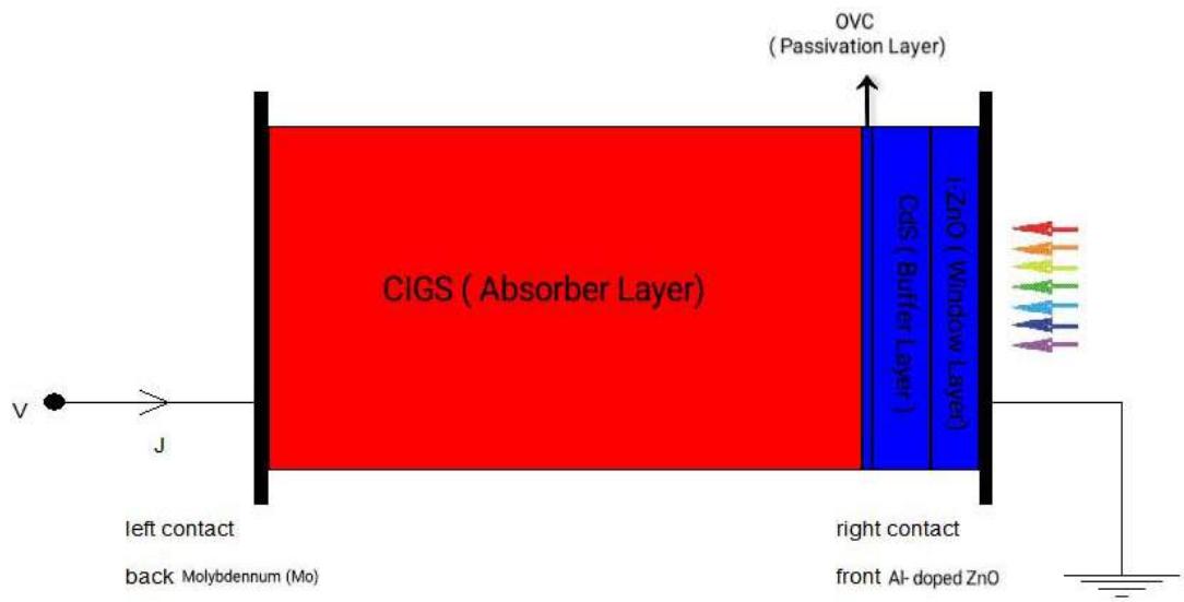 Figure 1: Schematic of the CIGS-based thin-film solar cell simulated in SCAPS-1D
IV. RESULT AND DISCUSSION
4.1 Effect of Absorber Layer Thickness on Solar Cell Efficiency
To evaluate the influence of the absorber layer thickness on device performance, the CIGS thickness was varied while keeping all other parameters constant. The band gap was fixed at 1.2 eV and the simulation was carried out under standard test conditions (AM1.5G illumination, 1000 W/m , 300 K). The thickness of the CIGS layer was varied from [0.800] m to [2.00] m in steps of [0.2] m[15]. The result shown in the figure 2, As the thickness increases: Jsc (Short-Circuit Current Density) rises due to an increase in the optical path length, allowing more photons to be absorbed across the solar spectrum. Thicker layers generate more electron–hole pairs, increasing the photocurrent. This trend continues until most usable photons are already absorbed and further thickness yields diminishing returns [16]. Voc (Open-Circuit Voltage) exhibits minimal variation. Voc is logarithmically related to the ratio of photocurrent to reverse saturation current. While photocurrent increases with thickness, the reverse saturation current also increases due to enhanced bulk recombination in thicker layers, stabilizing Voc.
{"image_source":{"path":"images/4c8f4b0cc9653c8728f521664786974b51adcdc368eff72869eaf8df5ab9eb18.jpg"},"content":"","chart_caption":[],"chart_footnote":[]} {"image_source":{"path":"images/f409dbb604b41b5ea85c7980c20dfb0bf2047a953dd657b8c6e6efdbf2827f4b.jpg"},"content":"","chart_caption":[{"type":"text","content":"Figure 2: Simulated variation of Jsc, Voc, efficiency and FF with CIGS thickness"}],"chart_footnote":[]}
FF (Fill Factor) improves initially due to reduced series resistance and better carrier transport in moderately thick layers. However, with further increase, the longer diffusion lengths required for charge carriers to reach the junction result in higher recombination, limiting FF improvement. Efficiency increases and reaches a peaks at 15.43% for a 1.6 m absorber thickness. Beyond this optimal thickness, recombination losses in the bulk outweigh the benefits of increased photocurrent generation, leading to a slight decline or saturation in efficiency .
4.2 Effect of absorber bandgap on solar cell performance
To analyze the influence of the absorber material's band gap on device performance, the band gap of the CIGS layer was varied from to , in steps of , while keeping the thickness fixed at . The simulation was conducted under standard conditions (AM1.5G spectrum, , 300 K)[18].
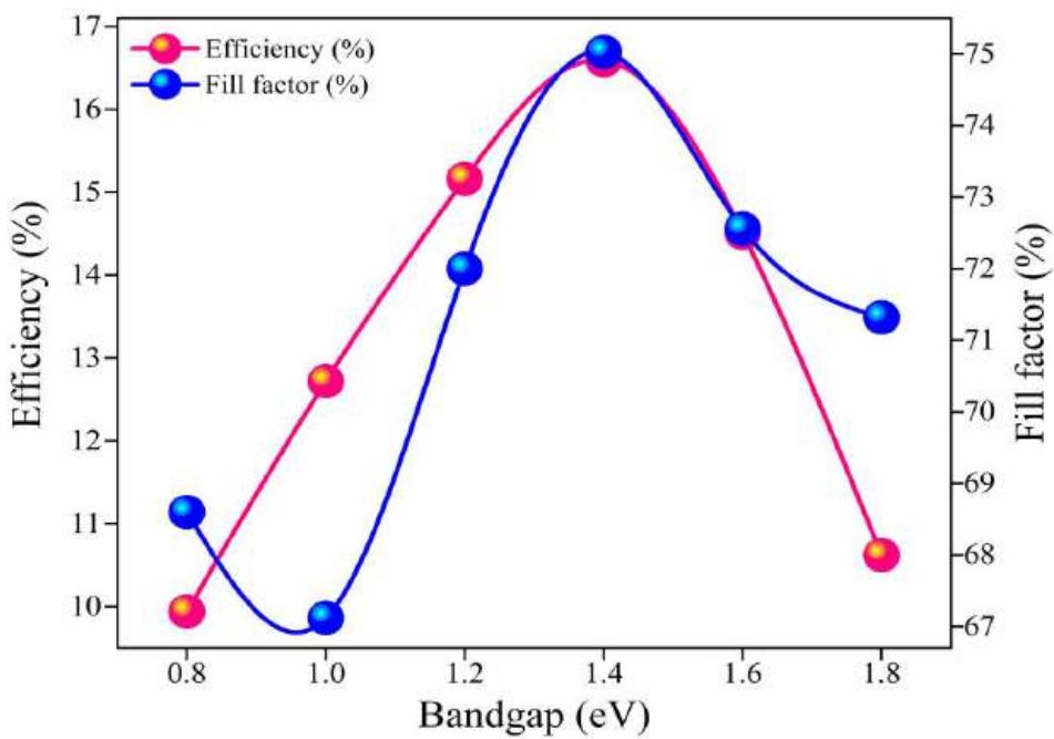
As shown in Figure 3, the power conversion efficiency increased with the band gap from 0.8 eV to around 1.3–1.4 eV, after which it declined. As the band gap increases, the Voc increases as well. This is because Voc is directly related to the difference between the quasi-Fermi levels of electrons and holes, which becomes larger in materials with wider band gaps. Additionally, a higher band gap reduces the intrinsic carrier concentration, thereby lowering the reverse saturation current and contributing to a higher Voc[19]. The fill factor (FF) also improves with increasing band gap, particularly up to the optimal range of 1.3–1.4 eV. This is primarily due to reduced recombination and more favorable diode characteristics. As the Voc increases and series resistance effects become less dominant, the FF benefits from improved charge extraction efficiency and lower losses in the J-V curve slope near the maximum power point.
However, Jsc decreases with increasing band gap. Although higher band gaps result in better voltage performance, they limit the absorption of lower-energy (longer-wavelength) photons. As a result, fewer photogenerated carriers are created, reducing the current output. This trade-off between increasing Voc and decreasing Jsc is a well-established characteristic in single-junction photovoltaic devices. The overall efficiency follows a non-linear trend, increasing with band gap until a peak is reached (around 1.3-1.4 eV), where the combined effect of optimal Voc, sufficient Jsc, and high FF yields maximum power output. Beyond this point, the loss in Jsc due to reduced spectral absorption outweighs the gains in Voc and FF, leading to a decline in efficiency[20].
The simulation results indicate that an optimal band gap lies between 1.2 eV and 1.4 eV, where the trade-off between voltage and current is balanced, leading to maximum efficiency. This observation agrees with reported values in the literature for CIGS solar cells, where a band gap near 1.3 eV is often cited as ideal for single-junction devices[21].
{"image_source":{"path":"images/f18425b99ea26cd7305d342e60302589cb71dd8d3e14c2f3ede51dc0b3f853ee.jpg"},"content":"","chart_caption":[],"chart_footnote":[]} {"image_source":{"path":"images/f0f3a868d841f237d3c953e1e50660e22c7fe0cd38fda87656172e439a11ab53.jpg"},"content":"","chart_caption":[{"type":"text","content":"Figure 3: Simulated variation of Jsc, Voc, efficiency and FF with bandgap"}],"chart_footnote":[]}
4.3 Effect of Operating Temperature on Solar Cell Efficiency
To assess the impact of temperature on solar cell performance, simulations were carried out over a temperature range from 240 K to 360 K in steps of 20 K, while keeping the CIGS absorber thickness fixed at 1 m and the band gap at 1.2 eV. The results, presented in Figure 4, show a clear decrease in efficiency with increasing temperature .
{"image_source":{"path":"images/2248aa4b1493d8a8d6ddc7c438f985fda03a941c6ba1f35720dbfa336c2aef1c.jpg"},"content":"","chart_caption":[],"chart_footnote":[]} {"image_source":{"path":"images/b3042773f58723d4cb2645eb62ac1b89bc3a3183ba665fbf5ff951a41646cc52.jpg"},"content":"","chart_caption":[{"type":"text","content":"Figure 4: Simulated variation of Jsc, Voc, efficiency and FF with temperature"}],"chart_footnote":[]}
At lower temperatures (240 K), the device achieved its highest efficiency. As the temperature increases, the open-circuit voltage (Voc) shows a noticeable decrease. This is due to the temperature-induced narrowing of the semiconductor band gap and the exponential increase in reverse saturation current, which lowers the built-in potential. The relationship is governed by the diode equation, where higher thermal energy leads to increased carrier excitation, enhancing recombination and reducing the maximum voltage the device can sustain under open-circuit conditions[23].
Similarly, the fill factor (FF) decreases with rising temperature. Elevated temperatures increase carrier recombination and series resistance effects, while also degrading the ideality of the diode characteristics. As a result, the shape of the current-voltage (J–V) curve becomes less optimal, lowering the FF. On the other hand, the short-circuit current density (Jsc) exhibits a slight increase with temperature. This is because higher thermal energy can enhance carrier generation and mobility to a limited extent[24]. However, this gain is modest and insufficient to overcome the larger losses in Voc and FF. The efficiency drops accordingly, as it is a combined outcome of Voc, Jsc, and FF. The loss in Voc and FF more than compensates for any minor gain in Jsc, resulting in a net decline in power conversion efficiency at higher temperatures. These trends confirm that thermal effects are detrimental to solar cell performance, primarily due to increased recombination and degraded voltage behavior. Therefore, proper thermal management and material engineering are crucial for maintaining the efficiency of CIGS-based devices, especially in hot environments or under high-intensity illumination.
{"image_source":{"path":"images/7edf9247da52334c12e2e62a19cdfe6f2a99f34d59a04c3e1add7e278be9c7e0.jpg"},"content":"","chart_caption":[{"type":"text","content":"Figure 5: I-V curve of the champion device"}],"chart_footnote":[]}
4.4 Quantum Efficiency Analysis of Optimized Structure
After evaluating the effects of absorber layer thickness, band gap, and temperature, the solar cell was simulated using optimized parameters: CIGS thickness = 1.6 m, band gap = 1.4 eV, and temperature = 240 K. The resulting quantum efficiency (QE) curve is shown in Figure 6.
{"image_source":{"path":"images/7b6f34788f4e71783149bcdadf77c6200c76648bf9a42de7b59d1f4fa7c2490d.jpg"},"content":"","chart_caption":[{"type":"text","content":"Figure 6: Stimulated quantum efficiency (QE) curve of the optimized solar cell (CIGS thickness = 1.6 "},{"type":"equation_inline","content":"\mu"},{"type":"text","content":" m, band gap = 1.4 eV, temperature =240 K)"}],"chart_footnote":[]}
The QE represents the fraction of incident photons converted into charge carriers at each wavelength. The curve exhibits a broad and high quantum efficiency, peaking above 90% in the wavelength range of approximately 350 nm to 900 nm, indicating excellent photon absorption and carrier collection in this range. At shorter wavelengths (below 400 nm), a slight drop in QE is observed due to surface recombination and absorption in the window/buffer layers. At longer wavelengths (>800 nm), the decline in QE is attributed to the limited absorption depth in the absorber layer for low-energy photons[25]. Overall, the QE spectrum confirms that the optimized CIGS solar cell structure exhibits high collection efficiency over a broad portion of the solar spectrum, validating the effectiveness of the chosen material and structural parameters.
IV. CONCLUSION
This study examined how variations in the CIGS absorber layer—specifically its thickness, band gap energy, and operating temperature—affect the efficiency of thin-film solar cells. Through a systematic simulation-based approach, it was found that each parameter plays a critical role in determining the device's overall performance.
The results showed that increasing the absorber layer thickness enhances light absorption and current generation up to an optimal value of 1.6 m, beyond which efficiency saturates or slightly declines due to increased recombination losses. Band gap tuning revealed that an energy gap of 1.4 eV strikes the best balance between voltage and current output, resulting IN improved efficiency. Temperature analysis showed a clear inverse relationship between operating temperature and efficiency, with the highest efficiency of 19.95% recorded at 240 K, confirming the negative impact of thermal recombination on photovoltaic performance.
Overall, the findings highlight that careful optimization of absorber layer properties is essential for achieving high-performance CIGS solar cells. These insights provide valuable guidance for designing cost-effective and efficient photovoltaic devices for real-world applications.

Great Britain Journals Press membership is an elite community of scholars, researchers, scientists, professionals and institutions associated with all the major disciplines. Great Britain memberships are for individuals, research institutions, and universities. Authors, subscribers, Editorial Board members, Advisory Board members, and organizations are all part of member network.
 For Authors
 For Institutions
 For Subscribers
Author Membership provide access to scientific innovation, next generation tools, access to conferences/seminars/symposiums/webinars, networking opportunities, and privileged benefits. Authors may submit research manuscript or paper without being an existing member of GBJP. Once a non-member author submits a research paper he/she becomes a part of "Provisional Author Membership".
Society flourish when two institutions Come together." Organizations, research institutes, and universities can join GBJP Subscription membershipor privileged "Fellow Membership" membership facilitating researchers to publish their work with us, become peer reviewers and join us on Advisory Board.
Subscribe to distinguished STM (scientific, technical, and medical) publisher. Subscription membership is available for individuals universities and institutions (print & online). Subscribers can access journals from our libraries, published in different formats like Printed Hardcopy, Interactive PDFs, EPUBs, eBooks, indexable documents and the author managed dynamic live web page articles, LaTeX, PDFs etc.
Conflict of Interest
The authors declare no conflict of interest.
Ethical Approval
Not applicable
Data Availability
The datasets used in this study are openly available at [repository link] and the source code is available on GitHub at [GitHub link].
Funding
This work did not receive any external funding.
References
Cite this article
Related Research




Special Issue
Launch a focused special issue to highlight research, emerging trends, and expert insights in your academic field.
